DIY VIA plating - Explained how copper gets inside of a VIA | Kailey Shara |

ฝัง
- เผยแพร่เมื่อ 15 มิ.ย. 2024
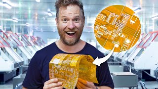
- Thinking to manufacture PCB at home? You may want to know how to put copper inside of a VIA.
Watch the full interview here:
- How Does Copper Get Inside of a VIA Hole in Your PCB - Do you know this? • How Does Copper Get In...
------------------------------------------------------
Would you like to support me? It's simple:
- Sign up for my Hardware design and PCB Layout online courses: academy.fedevel.com/
- You can also support me through Patreon: / robertferanec
- Or sign up for my Udemy course: www.udemy.com/learn-to-design...
It is much appreciated. Thank you,
- Robert


She is very smart and speaks well. I also just found your channel for the first time. I am going to watch, like, subscribe and then again the full video later!
It is so much more complicated that I expected.. I might give it a try though haha
I am wondering how much better this performs compared to like copper/thermal pastes that turn into solids?
it definitely better ita industrial technique
For me it's better to solder a hook-up wire on both sides of the via hole to the two pads :) p.s. Why don't you continue with the 100 hardware design tips playlist?
Same here. I use my old LPKF router to drill 0.3mm holes in 0.75 VIA pads. I insert 30 gauge wire wrap wire through each hole, bend the end over on the far side and then bend and trim with an OLFA art knife on the insertion side. I then trim the wires on the far side after all the VIAs are done. I then solder all the wires to the VIA pads on each side. All done using a stereo microscope. Much faster than using rivets. I minimize the amount of VIAs employed during the PCB layout.
How work in collaboration
Watch the full video instead!!! Full videos are always awesome, and are for smart people / people who want to get smart. Excerpts and shorts are for dummies!!!
I wouldn't say they're for dummies. I watched this short video at first, and then watched the full video as I was hooked by the subject.