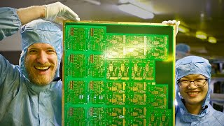
Plated Through Hole Printed Circuit Board Fabrication

ฝัง
- เผยแพร่เมื่อ 13 ต.ค. 2015
- The University of Manchester offers a PCB fabrication service to students and staff. This video documents the process and highlights limitations when preparing designs.


Excellent and thorough video, well done!
really interesting, I had no idea just how many steps there were, so many baths!
+Sam Walsh And machines.
Hi. As the machine is called? to find more information about it!
Hello @FSE elearning can you please send the details of machines/models which are used in this lab
Nice video thank You!
Can you tell please the catalyst and acceleration solution right ingredients?
Why do you not micro-etch before catalyst?
All the time all the holes plated well?
Thank You
Ferenc
the process of plating the holes on a piece of FR4 material is is very reliable, until the first 4 baths have had an amount of material through them, after that you will find the odd holes not plated, which is easy to see when you hold the finished plated board up to a light source.
Normally baths 1,3 and 4 are the ones that would make the through hole plating fail. Running the pcb through all the baths again for half the specific time rectifies the non plated holes.
Then a chemistry change of those baths with get the system back up and running.
Silkscreen must be added to this spectacular process
Where can buy this machines?
How are the plated holes not destroyed in the etching step?
Is this missing a step that protects them, or is it some kind of selective voodoo etching process?
Each layer has it's own mask - the film applied is protecting the holes.
the photo resist film protects every hole that is aligned up
Where could I get the information of the components in each tank?
Thaks
I just replied to Ahmed Bilal, who asked the same question, please read the reply.
Which chemicals/process I can use, if I want to do PTH , at home ?
I just replied to Ahmed Bilal, who asked the same question, please see this reply. :)
Why so many out of focus shots? So annoying!
This was interesting but NOBODY in the real world can use these processes... unless they work in a PCB fab shop (or are students at the U of Manchester apparently)
Thanks for the comment - the video is intended as a resource for UoM students but was made public for general interest.
If you search around TH-cam enough like I did, then yes, you and anybody in the real world can use these or similar processes to make a PCB.
yes! me too
No wonder there is a huge gap betweeen University and real world engineers.
Which chemicals/process I can use, if I want to do PTH , at home ?
You probably already know how to etch the top and bottom - if not, let me know.
Right after you've drilled the holes, you'll want your holes plated.
Short answer: "Conductive silver ink" and "copper sulphate" are the basic chemicals you'd need. The conductive silver ink can be replaced by some other conductive paste or fluid, depending on what you can get.
Copper will not bond to the fiberglass itself, but it will bond to something that's electrically conductive.
So you need to, somehow, make the inside of each hole electrically conductive.
You could do the following:
1: Place a sheet of stiff transparent plastic on a completely flat surface.
2: Place the drilled PCB (with its burrs removed) on top of the plastic sheet.
3: Using a syringe with a needle-tip, fill each hole with conductive ink
4: Remove the conductive ink from each hole, so there's room for the copper plating.
5: Let the conductive ink dry.
6: Get rid of the conductive ink that's not inside the holes.
7: Finish by using a copper-plating bath, there are many copper-plating videos on TH-cam, I'll mention a few below.
For the copper bath, you'll need copper sulphate (in the US, you should be able to get "Root kill" or "Root away" which is very cheap, I'm not that fortunate, as I'm from outside the US).
Example video on copper-plating (this is a PCB plating video):
th-cam.com/video/KTNuTv_IQp4/w-d-xo.html
(I believe his home-made conductive ink is quite expensive).
General copper electroplating video:
th-cam.com/video/T3qhqTVssoo/w-d-xo.html
Those two videos might be enough for you to succeed your first PTH process.
-Make sure your electrodes are thick copper rods (don't use any other material, as other materials will contaminate the plating; eg. nickel electrodes would make your plating part copper part nickel).
The plating voltage is very low (usually below 7V DC).
Notice that you'll need to regulate the current.
It'll be helpful to get one of the cheap step-down converters that have a "Constant Current" feature.
Make sure both your AC-to-DC PSU and your step-down converter can handle the current you want to draw from it - you may get away with using lower currents, but it will take longer to do the plating.
Note: You can use the syringe to fill a hole, then suck the ink back up into the syringe; this will save ink and it will probably also make sure that the ink does not dry too quickly.
Conductive silver gives you the advantage of being able to check if each hole has ink inside it; place a light on the oposite side of the PCB, hold the PCB in your hands and tilt it back and forth (look at the PCB from an angle); if the hole easily reflects the light (like a mirror), then it contains ink. If it does not contain ink, then it looks darker than the others.
If you want to take things two steps further, find yourself some UV-curable liquid soldermask (for instance red and white from ebay), then you can add soldermask and silk-screen to your PCB. I've seen people use nail-polish for silk-screen (it's likely cheaper than the UV curable soldermask). The key to a good result here, is to use a transparent sheet of plastic to push down and spread the soldermask paste evenly.
Finally, If you only need to do a single PCB, you might want to skip the plated-through-hole process and stick pieces of wire through each hole, solder on both sides, it's lo-tech, not so messy and also cheap - but it doesn't look as cool of course. ;)
Note: The 'pre-dip' used in this video (palladium colloid) isn't really affordable for hobbyists.