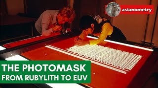
Photomasks Explained (Contact and Projection): how to etch Thin Chromium Layers
ฝัง
- เผยแพร่เมื่อ 29 ส.ค. 2024
- In this video, the difference between contact/proximity masks and projection masks for photolithography is discussed. These masks are used to produce MEMs and integrated circuits. In the second half of the video, I will show how to quickly etch the chromium layer off a quartz substrate.


This Channel is pure Gold. Thank you very much for sharing those rare insights
big fan of all your videos, thank you for putting out such well explained and detailed content!
It is very unusual to see somebody handles a mask without gloves ☺️
Thanks for putting this together. Very educational.
very smart way to remove Chromium, thank you for sharing.
I bought a quartz photomask from a 1998 TSMC batch. I bought on Ebay. Its my favorite trinket.
I had got some masks to try and remove the chromium from. Found a Q-switched 355nm laser worked nice, ablated the chrome while leaving the quartz untouched, though this slow to the point to being useless. I ended up using the mask as a work surface in my furnace.
I have a question:
Is there any significant lens between the photomask and silicon wafer during the lithography or patterns of photomasks are real size? I think we can't design life-size patterns on the surface of photomasks because as you said, the scale that we're talking about is in order of nanometers!
That's a very cool hack for a fume cupboard ! Really interesting about how the Pellicle de-focusses dust particles; reading about pellicles in semi-conductor / chip manufacturing I get a lot of oddly conflicting information (will eventually did deeper). In my 20's I did a lot of odd chemical mixing under heat that looking back I shake my head at. Is it possible to lap the Chromium layer off a quartz plate ? I know some fiducials on plates can be (skillfully) removed with a scalpel. And not to ask too many questions how do you / one know if one has a glass plate or a quartz plate ? Is there a quick test for that / tell tale signs before one has to measure refractive indices or analyze spectra etc. ? Thanks again for making these amazing videos.
Hi ED, Thanks for you feedback. Yes it is possible to lap off the quartz. If you use rough lapping, it will be gone very quicky, but you will end up with a "frosted" window surface. If you use the "polishing" type of lapping, removal takes a long time. About quartz and glass: First you can find the code indication on the mask carrier box, second you can look at absorption (quarz has low absorption up to 190nm) and third you can look at thermal expansion coefficient on a hot plate using a micrometer gauge to measure the expansion during heating or cooling down. Quartz has a much lower expansion than borosilicate or float glass.
@@HuygensOptics Hey , thanks for that , wouldn't have thought of mapping out the thermal expansion, NICE tip ! Does make me look at Quartz with "New eyes". Very useful material.
I have this question Huygens optics, how on earth this they made those billions of transistor patters in that photo mask. Thank you for the video.
how on earth did you manage to get those masks
Where would one get his hands on some liquid photoresist suitible for this kind of thing?
i have designed my devices, how to make mask for my devices. Is it possible to make mask using laser writing? i want to make mask for mask aligner. kindly suggest?
Very interesting! What wavelength do you think was used for the original mask, EUV? Your video as always was great.
A chip is a combination of both duv and euv light. Duv do the lower layers while euv is introduced in the last few complicated layers
Ammonia is a weak base, but very powerful when concentrated ;-)
Thanks for this video)
Why do you have such thick missive granite table?
It's likely a "surface plate", commonly found in engineering and machining workshops, part of the process for making things flat or square.
Why did you not use a Standart Cr-etch as it is sold at microchemical for exampel?
But how is the first one made? I mean so lets say they designed a new chip. How would they take that CAD version of it and write it to the wafer? I dont understands.
The masks themselves are generally written using e-beam lithography. This is a very accurate process that takes a long time, so it's not suitable for chip manufacturing itself. But it is suited for mask manufacture.
@@HuygensOptics Just to understand you. So the microscopic circuitry that we always see on microscopes is drawn that way? Thats the point the chips go from software to hardware?
As i was listening to this I was wondering whether I've ended up at at the right channel, apparently not
Why are you removing chromium from a sheet of quartz glass? Wht not buy a sheet of clear glass?
Because this is quartz glass which is generally more expensive when you buy it new then when you buy old photomasks.
Please wearing poly globe~