It's always interesting to see how much textile technology has guided computer technology. This is essentially the same process that is used in screen printing and even older wax resit methods(such as batik). And of course, jacquard looms are proto-computers.
This was an INCREDIBLE video!!! I have been helping a semiconductor fab do the CAD drawings for the new tool install so i spend a lot of time around all of these machines. I had no idea how they or what the process was but this totally explained it! Thank you!
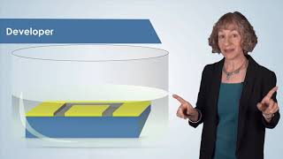
Nice! This series is a great introduction to semiconductor manufacturing. Lithography is an important part of the process, repeated many times to build a circuit.
Hi ! In the example used with Gold , isn't Gold a photoresist? Because you had the silicone, and then on top you need to have a photoresist directly, but there was Gold .. so is gold = photoresist ? Thanks for the video !
Thank you very much for the video. Could you tell me what are the possible causes of stitching lines? why some lith machine macke stitching line during the lith process an other machines dont have this problem? thank you very much!!!!!
You need to watch Huygens Optics latest video. Both the light source and the mask is needed to be designed/adjusted by counting the effect of the diffraction. So much in fact that both the light source pattern and the mask look like a diffraction pattern themself (-for layman at least).
Very good video. I'm still wondering though, if they use this process to get parts 7um thick, how do they get things down to 2nm? I read 1nm is 1000 times smaller than 1um so how do they get any accuracy at the nm scale? How do they manage to line everything up when when it's only tens of atoms wide... Also the wavelength of ultraviolet light is wider than these dimentions anyway so how is it even possible? My head hurts!


It's always interesting to see how much textile technology has guided computer technology. This is essentially the same process that is used in screen printing and even older wax resit methods(such as batik). And of course, jacquard looms are proto-computers.
This was an INCREDIBLE video!!! I have been helping a semiconductor fab do the CAD drawings for the new tool install so i spend a lot of time around all of these machines. I had no idea how they or what the process was but this totally explained it! Thank you!
this is exactly what i've been looking for and very thoroughly explained. thanks a lot!
A really wonderful explication of the complete photolithography process. Thank youuuuu.
You're very welcome!
this is excellent for beginners, it explains thing simply from the ground up, well done !!!
Wonderfully done, informative and well produced! Thanks for taking the time to create these and sharing them!
great
Very helpful, thanks for putting this on TH-cam!
Nice! This series is a great introduction to semiconductor manufacturing. Lithography is an important part of the process, repeated many times to build a circuit.
Glad you enjoyed it!
these are great short learning templates. Thanks for producing them
your explanation is awesome I had a problem to understand this part but I understand this from you despite I am not good in english so thank you
Nan makes me feel like a Neanderthal. Beautifully delivered talks / lectures, thank you.
Such content for free,thankyou
Great videos to learn about semi conductor processes
Great video. Really helpful!!!
Glad it was helpful!
Awesome content on Photolithography with the real equipment and quite nice explanation.. thank you so much guys! Keep it up!😍
Our pleasure!
thanks for the detailed information!
Hi ! In the example used with Gold , isn't Gold a photoresist?
Because you had the silicone, and then on top you need to have a photoresist directly, but there was Gold .. so is gold = photoresist ?
Thanks for the video !
perfectly explained! nice pace! beginner friendly
Thank you very much for the video.
Could you tell me what are the possible causes of stitching lines?
why some lith machine macke stitching line during the lith process an other machines dont have this problem?
thank you very much!!!!!
Very good explanation
thank you for such clear explaination
does diffraction soften the pattern when transferring the pattern?
You need to watch Huygens Optics latest video. Both the light source and the mask is needed to be designed/adjusted by counting the effect of the diffraction. So much in fact that both the light source pattern and the mask look like a diffraction pattern themself (-for layman at least).
Very descriptive. Thank u❤️
You’re welcome, glad it was helpful!
Great video, thank you!
I used this video to get a job I'm woefully under qualified for.
So useful thanks alot
Awesome
Thanks alot
Great presentation, shame about not showing the gold layer process though. I still learnt a lot though, thanks.
Thanks a lot, very good explenation
why do we need to inscribe patterns on the substrate??
where im gone get a cooking pan to make this dice ,taste the best ?
Very good video. I'm still wondering though, if they use this process to get parts 7um thick, how do they get things down to 2nm? I read 1nm is 1000 times smaller than 1um so how do they get any accuracy at the nm scale? How do they manage to line everything up when when it's only tens of atoms wide... Also the wavelength of ultraviolet light is wider than these dimentions anyway so how is it even possible? My head hurts!
by using ebeam lithography or direct write lithography
Fletch! #POW
You deserve to get my school fees.
Ktu students like adi
Deepak kalal OP
Experience some natural and art today 🫡