It's incredible how you can explain these incredibly complex topics in a very approachable way. You just explained etch to me in a way that makes sense. Etch has always been a certain flavor of magic to me. Thanks!
13.56 MHz turns out to be the exact same frequency used by credit cards and bus passes. Is that a coincidence? Edit: turns out it's in right in the middle of an ISM band so you don't need a licence to install a tap to pay reader on a gas pump, just like you don't need a license for your microwave oven even though it is designed to emit radio waves. If you tried 15.00 MHz you'd probably cause all the nearby shortwave radio clocks to go out of sync and the FCC would get mad at you, which is generally something to be avoided.
No coincidence. The 13.56 MHz band is an official ISM (industrial scientific medical) band which allows providing low (and high) power RF energy into a load. External and out-of-band radiation is severely frowned upon by others including FCC. Much more info available, consult Google.
This is exactly correct. More cowboy engineering in action. The engineers who invented plasma etch used 13.56MHz because it combined RF generators that were commercially available off the shelf with license-free use.
THat's right - 13.56MHz is used because of FCC radio frequency allocation rules, not (as I thought for years) that it must be the "magic plasma frequency" - has nothing to do with physics, but instead gov't policy, haha! Engineering...so many moving parts.
This is probably the best video I've seen for an Intro to Dry etching. I actually appreciate that the ions, plasma and chemistry physics are *not* included - this is a fantastic intro after which someone can then delve into how plasma and ICP's work. I'm sending this to our undergrads!
You should, in fact, NEVER shake a Polaroid picture. Moving the developer around will massively interfere with the process and reduce quality of your picture. The Polaroid company recommends to place the picture on a flat even surface.
correction: @12:00 the lazor shark, was spotted actually in Florida. It was also one of those rare instances that, the camera survived, but the camera man... well... became chum, if you catch my sea drift there.
Your photo of the "Electronics" article reminds me of the joy of reading magazines. In college, I would go to the library and read technical magazines.
Fantastic content. I worked as electronics tech in Microns RD etch fab in Boise in early 2000s. We were qualing 12inch tools, doing some copper trials on 8" . Did some high dielectric testing also. That fab had Lam Tel and applied all in about 1/3 ratio. Older 8" applied were heavily modified to do interesting etches. Thanks for your time and the content. The history you cover and your style is excellent.
I have always understood that we use isotropic and anisotropic etching. You did a great job as usual explaining the progression of semiconductor etching.
Since there is a lot of work going in to exploring manufacturing of wafers and such in Zero-G, it would be really interesting to see you discuss all of the R&D going on with manufacturing in space and the advantages Zero-G manufacturing would give. Thanks! Your knowledge and research on these subjects is really amazing and I would really appreciate it if you could leverage your unique skillset to explain all of the issues going on in this R&D space in space.
17:12 Sorry, but Nvidia does not have any stacked die products yet. They took out a patent on their flavour of it in late 2021, but has not brought it to market yet. HBM is the only industry standard component that uses die stacking, and Nvidia does use those (just the same as AMD and Intel), but they're produced by Micron, SK Hynix or Samsung. The only other product that uses die stacking is the AMD chips that end in "X3D". I felt that was a needed clarification as the wording "die stacked chips like our modern Nvidia AI accelerators" was unclear to the point of being misleading.
Memory serves up a 1960's Playboy cartoon showing a well dressed gentleman inviting,, (luring), a voluptuous young lass to accompany him, with the caption reading: " Would you care to come upstairs to my loft and see my etchings ? "
While it’s obsolete for silicon technologies, resist undercut is extensively used as a desirable feature of liftoff patterning where gold is used to carry current (gold has no volatile halides, so it cannot be dry etched). This is still very common in GaAs power amplifier technologies.
Technically anything can be dry etched if the power is high enough. Saw someone sputter gold with nitrogen in a RIE once. But of course that's sketchy unless you really need super fine gold lines.
@@tykjpelk sure, if you don’t mind sputtering gold all over everything and failing reliability testing. What works in a university lab or a white paper to get a pretty SEM image rarely works in the field.
@@Grak70 It's absolutely not something you'd want to do for anything CMOS, at least in FEOL. I think this was done for MEMS, and indeed probably not anywhere near production.
@@tykjpelk well you certainly wouldn’t do it for silicon CMOS in any case. Gold contamination forms trap states in the silicon bandgap. You can’t have gold anywhere near a silicon fab.
@@Grak70 That's certainly true. I've read a bunch of papers on gold etching with IBE from back in the 70s, but now when I look them up it seems they're all about GaAs or SAW devices.
Your videos are such a great resource to get an idea / an understanding of todays high-tech. Thanks! It is amazong how electronic tech evolves since almost 60 years. And the history is very interesting as well. As we scratching the limits of atomic strucktures/layers I wonder what R&D ideas are present to overcome this and what is the future of chipmaking?
forgot about etch in semiconductor manufacturing,didnt knew there are so many processes in used (i knew oonly about rie and wet etch). Cant wait for next etch vid
Cant remember magnet ring on Lam but Applied had static electro magnet ring and energized them in series, Tel had fixed magnets and mechanically spun them. Interesting to see same process on different tools and setting required for similar outcomes.
Wow, Jon, this was particularly interesting! When you need another good story to tell, how about expanding on Tracer Lab? Some special expertise and situations there! 😎✌️
5:55 13.56Mhz is the carrier frequency used by NFC smart cards (credit cards among others ) to power the card. It's modulated to transfer the data. Any reason why this frequency is used in both cases?
I don’t know why NFC cards would use that frequency, but the reason that it’s the standard frequency in plasma processing equipment is that that frequency is within the ISM bandwidth (specifically allocated for industrial, scientific and medical equipment) and that RF emissions in this band do not interfere with critical communication frequencies.
@@SuperCuriousFox I see this makes so much sense now. I design NFC readers for a living and was under the impression that the 13.56Mhz band was for us (some narcissism creeping in there). I guess that the when NFC was designed the designers from Philips and Sony chose that frequency, because knew that it would be free for the fields where NFC readers would be used. No one needs to pay for a coffee in the middle of an industrial plant or an operating room. I need to read up on the history of why 13.56Mhz was chosen for NFC. Thank you for the insightful reply. Have a great day.
Yeah, band allocation is the reason. A professor in my old group once modulated a high power signal, I don't know what, to some random number well into the MHz. Not too long after the university was contacted by the local air base who told them to knock it off.
Because that part of the radio spectrum is allocated to exactly these kinds of devices. 13.56+/-0.007Mhz is one of the so called “ISM” bands reserved for “industry, science, and medical” use. As such, there are no licensing requirements to use it. Although it’s possible to broadcast and receive in that band, machines that do so typically don’t exist since your data would be corrupted every time someone within 100ft microwaved a burrito.
Gotta find that shark graphic… It won't fill the hole of never managing to get a job doing what I studied at University, but at least I can come here and get filled in on what happened in the intervening 20 years.
I really love your videos on explaining all the steps involved in making semiconductors in really great details, but i am always disappointed by our outtro which feels like you have to meet a certain deadline and need to rush through your last lines to subscribe,like and share etc. to be honest, that rapid change of speed is a bit offputting. I was pleased in your last video to hear it in a calm matter which i really enjoyed (besides the video itself of course). I think it would be more pleasant if you take your time for each video to close them the same way you did last time even tho i might take a couple of seconds longer. Keep your great work up :)
I think you should try to go for live-action in-person reporting at a fab. Yeah, it's hard for the average person to get acess to such facilities, but you have a channel with half a million subscribers, you're a "reporter", whatever that means in the 2020s. It's doable, and would doubtless take the channel to heights undreamt of.
This might be difficult because of the sound of a fab. We have to basically yell at eachother when we're in the fab to communicate, so I dont know how enjoyable it would be to watch a longer video from inside the fab. I'm not a huge fan of Linus Tech Tips but he does a fab tour and he has to basically yell at the top of his lungs the entire time he's in there.
Takes me back to MOS4, the 03 photo bay... had certifications (the little Tyvek card) for all processes. There was a Tegal across the way on the diffusion side... it make a big SPAK!! noise when it was used.
Thks &; 1. ?Is light the only means/tool tha can map out the areas to etch? 2. If-so, ?Can a laser of appropriate frequency be used to directly etch silicone?
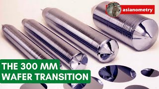
The story of the 450mm transition debacle would make an interesting video, billions were spent on an 'obvious' next step, moving from 300mm to 450mm, but it never happened, 3D deep tunnel etch and sub 5nm proved too efficient I guess.
Could you possibly make a video about the step-by-step process of making a chip? Like starting from the silicon being drawn into that giant single crystal turd of (nearly)pure silicon to the different steps of the lithography and etching and all that complicated jazz that eventually forms the wafer into the chip that gets cut then diffused or whatever to the substrate and everything else until I pop it in my mobo and fire up Asianometry on TH-cam??? LOL I KNOW it's a LOT and there's NO WAY you would ever be able to find out every step, trade secrets and all, but I'm not saying every single step... just the different types of steps the wafer goes through.... ANYWAY.... if you were already working up to putting all your separate videos on the semiconductor creation process and making us use all that knowledge when you present to us your magnum opus: 'The Entire Semiconductor Creation Process' (or something along those lines) You've covered so much of it already that I feel like you HAVE TO be working towards making this video. And because I don't know the steps in the process I keep expecting that video to be the next one lol I don't expect you to tell me if you are doing this, but if you hadn't made this your plan then please consider it. It would be a really good video because you will be able to refrence all the past videos you've done about the big steps of the process. But if you do make this then I REALLY think you should try to play nice with the youtube algo and make a catchy title like "Every piece of the modern world relies on THIS little known process" or one of those TERRIBLE CHEESY titles that the algo NEEDS to see/read in order to put it in front of other people's eyeballs... but you also HAVE TO make a certain type of catchy thumbnail too... the problem is that right now that algo wants to see a face, preferable with an astonished or overly surprised look (you know the one lol) But I know after hearing you talk about this on an interview (I THINK it was you and you were talking with Tom on Moore's Law Is Dead.. I could be totally wrong tho lol) that you don't want to do things like this and it's not your style (I feel really stupid right now because I'm getting the feeling none of this was from you 🤦♂ lol oh well ) WELL I think that if you did make that video then you SHOULD kowtow to the TH-cam AI algo because that would be the one vid that shows off a lot of YOUR work and the topic that YOU are MOST Interested in... so you would get a lot of new sub of people that have your same interest, and real fans of your work that want to learn about the SUPER COMPLEX parts of our modern world that (barely) work to make it all happen.
Is it possible to etch with light? Surely that’s the way to go if moors law is to keep progressing? Please cover X-ray lithography too that requires a syncatron source
It's amazing that we can make these amazing machines, i wish alan turning was around to see what we can do now also if we ever found alien tech we would need their alien Lithography tech
It would be very interesting to make a video about the Gallium them. Galliumnidrid is beside Siliziumcarbid an advanced semiconductor material. It allows higher voltages and faster switching than traditional silicon semiconductors. Siliciumcarbid is made from Sand and Coal. It is everywhere cheap available. But Gallium becomes extracted from Aluminium. It is a very energy and pollution intensive process where China has a de facto monopol on it. LEDs are only realizable with GaN. So the preferation of LED bulb monopolizes and reinforces Chinas world hegemony. The EU had forbidden traditional light bulb like Tungsten or Mecury/Phosporus bulbs. The effect was the death of the German OSRAM and the Dutch Philips Light concerns. The entire light industry was given to China with their Gallium LED monopol. In the USA Sylvania etc. was crashed in the same manner. For some semiconductes GaN are also difficult fo replace with SiC. But the entire western world becomes either completey dominated from China or frees from Gallium dependence. Meaning to reastablich domestic Tungsten / Mercury light factories and avoiding GaN in all Semiconductor applicances where SiC or simple Si can also be used. Would really be very intesting to make an video on this topic !!
In practice you always trade selectivity for directionality. A heavy non-reactive ion like argon will etch straight down, but it won’t distinguish between layers and the etch products will sputter rather than diffuse away from the surface. Purely chemical reactive species with low ionization will be very selective, but won’t interact with the plasma electric field strongly, so they will etch isotropically like a wet etch. In practice, you either alternate etch chemistry to form a passivation layer that prevents isotropic etching or strike a balance between etch species to achieve the profile you want.
A major part of my PhD was on ICP-RIE using argon, which is non-reactive. Everyone who knows their shit might be asking themselves why I would do something like this. So, the big idea is that you get sputtering only. That's basically like chipping away at the material with tiny hammers. In principle it's very anisotropic because all the atoms go straight down. It's also able to etch materials that don't react with etching gases, like many metals, LiNbO3, or in my case, potassium lanthanide tungstates. The downsides are: 1: Redeposition. When you sputter away atoms, they go somewhere. That could be sideways, right onto the mask, and onto your structure. So you lose resolution, the structure is coated with amorphous whatever, there might be extra sidewall roughness, and your structure will look like a medieval castle with crenellations, because the redeposition also coats the mask. Back in the day they used ion beam etching, and this was one of the major issues with it. ICP-RIE still has that, but at least it's way faster. 2: Physical etching is not very selective. You want to be able to use a mask material that isn't etched, because then you can do lithography on something super thin, and that makes it easier to get good resolution. In my case, I got a selectivity of 3:1. In some other processes in our cleanroom, we had 50:1. 3: Reticulation: Basically it destroys photoresist. I don't remember why, but it's well established that in pure sputter etching, polymers deform, bubble, crack and harden. You'll get roughness, etching where you don't want to, and a layer of ultra-hard polymer bullshit that fuming nitric acid can't touch. So that's why you don't want to go this route unless you really have to. However, if you want more physical etching there are ways to do that. For example, in ICP-RIE you can use more RF power and less ICP, meaning you have more intense physical bombardment. You can also add more argon, or make other changes to the chemical mixture like more or less SF6.
Hey man, long-time viewer/first-time (I think?) Commenter...AND NOW FOR SOMETHING TOTALLY IRRELEVANT - is it 1 newsletter every one or 2 wks, or one or maybe 2 Newsletters/wk? I know it's a small thing, but it really bugs me I can't figure it out... ;~ ]
You have the most interesting videos on semiconductor manufacturing and electronics and you seem to know quite a bit about the subjects, but your pronunciation of DRAM, vias, anisotropic and other words are not in line with the way most people pronounce in the industry pronounce them. Do you have an EE background? Thanks for the videos.
Thanks for the vidja! As for FUSION.... Well.....we will have fusion someday... just not today.... maybe not next week....um.... or the week after. Anyway.. you should just get about your business and not worry about it... Let's leave it to the professionals... Yeah.... THAT'S THE TICKET! FUSION!!!! It's THE FUTURE!!!! (circa 1930... or 1940... maybe 1950? DEFINITELY 1980! REAL SOON NOW!) ***sigh***


Time to escape for 18 mins into the simple world of ic manufacturing from the very complicated real world.
My etching machines would never leave me 😂
@@lukeonuke But they might on occasion reflect your RF and extinguish the plasma between you.
It's incredible how you can explain these incredibly complex topics in a very approachable way. You just explained etch to me in a way that makes sense. Etch has always been a certain flavor of magic to me. Thanks!
Yeah, this is my new fave channel. It answers all the questions I have about these processes.
13.56 MHz turns out to be the exact same frequency used by credit cards and bus passes. Is that a coincidence?
Edit: turns out it's in right in the middle of an ISM band so you don't need a licence to install a tap to pay reader on a gas pump, just like you don't need a license for your microwave oven even though it is designed to emit radio waves. If you tried 15.00 MHz you'd probably cause all the nearby shortwave radio clocks to go out of sync and the FCC would get mad at you, which is generally something to be avoided.
No coincidence. The 13.56 MHz band is an official ISM (industrial scientific medical) band which allows providing low (and high) power RF energy into a load. External and out-of-band radiation is severely frowned upon by others including FCC. Much more info available, consult Google.
This is exactly correct. More cowboy engineering in action. The engineers who invented plasma etch used 13.56MHz because it combined RF generators that were commercially available off the shelf with license-free use.
Sounds fun
THat's right - 13.56MHz is used because of FCC radio frequency allocation rules, not (as I thought for years) that it must be the "magic plasma frequency" - has nothing to do with physics, but instead gov't policy, haha! Engineering...so many moving parts.
slowly but surely you will reach a million. your that smart friend i never had. thanks
Thanks!
4:40 almost spat out my coffee
This is probably the best video I've seen for an Intro to Dry etching. I actually appreciate that the ions, plasma and chemistry physics are *not* included - this is a fantastic intro after which someone can then delve into how plasma and ICP's work. I'm sending this to our undergrads!
You should, in fact, NEVER shake a Polaroid picture. Moving the developer around will massively interfere with the process and reduce quality of your picture. The Polaroid company recommends to place the picture on a flat even surface.
you know what to do
you know what to do
YOU KNOW WHAT TO DOOOOOO
And you should never blow in to a NES cartridge that doesn't work. But that never stopped anyone.
Whoo whoo! 😂
@@idrathernot_2 Lend me some sugar. I am your neighbor!
I used to blow on those cartridges every time.
correction:
@12:00
the lazor shark,
was spotted actually in Florida. It was also one of those rare instances that, the camera survived, but the camera man... well... became chum, if you catch my sea drift there.
I can't trust you because the camera man never dies!
Laser shark always leaves one survivor to tell the tale. Sometimes just the camera is enough.
Your photo of the "Electronics" article reminds me of the joy of reading magazines. In college, I would go to the library and read technical magazines.
Jeez,what's up with reading wank mags in college like most folks did?
Fantastic content. I worked as electronics tech in Microns RD etch fab in Boise in early 2000s. We were qualing 12inch tools, doing some copper trials on 8" . Did some high dielectric testing also. That fab had Lam Tel and applied all in about 1/3 ratio. Older 8" applied were heavily modified to do interesting etches. Thanks for your time and the content. The history you cover and your style is excellent.
I have always understood that we use isotropic and anisotropic etching.
You did a great job as usual explaining the progression of semiconductor etching.
Since there is a lot of work going in to exploring manufacturing of wafers and such in Zero-G, it would be really interesting to see you discuss all of the R&D going on with manufacturing in space and the advantages Zero-G manufacturing would give.
Thanks! Your knowledge and research on these subjects is really amazing and I would really appreciate it if you could leverage your unique skillset to explain all of the issues going on in this R&D space in space.
17:12 Sorry, but Nvidia does not have any stacked die products yet. They took out a patent on their flavour of it in late 2021, but has not brought it to market yet. HBM is the only industry standard component that uses die stacking, and Nvidia does use those (just the same as AMD and Intel), but they're produced by Micron, SK Hynix or Samsung. The only other product that uses die stacking is the AMD chips that end in "X3D".
I felt that was a needed clarification as the wording "die stacked chips like our modern Nvidia AI accelerators" was unclear to the point of being misleading.
Memory serves up a 1960's Playboy cartoon showing a well dressed gentleman inviting,, (luring), a voluptuous young lass to accompany him, with the caption reading: " Would you care to come upstairs to my loft and see my etchings ? "
I remember when you were able to buy bottles of CF4... good times.
9:55 "a hole that allows gas to come in and out of"
oh
so your dad?
While it’s obsolete for silicon technologies, resist undercut is extensively used as a desirable feature of liftoff patterning where gold is used to carry current (gold has no volatile halides, so it cannot be dry etched). This is still very common in GaAs power amplifier technologies.
Technically anything can be dry etched if the power is high enough. Saw someone sputter gold with nitrogen in a RIE once. But of course that's sketchy unless you really need super fine gold lines.
@@tykjpelk sure, if you don’t mind sputtering gold all over everything and failing reliability testing. What works in a university lab or a white paper to get a pretty SEM image rarely works in the field.
@@Grak70 It's absolutely not something you'd want to do for anything CMOS, at least in FEOL. I think this was done for MEMS, and indeed probably not anywhere near production.
@@tykjpelk well you certainly wouldn’t do it for silicon CMOS in any case. Gold contamination forms trap states in the silicon bandgap. You can’t have gold anywhere near a silicon fab.
@@Grak70 That's certainly true. I've read a bunch of papers on gold etching with IBE from back in the 70s, but now when I look them up it seems they're all about GaAs or SAW devices.
10:59 "1-1.5 micrometers" sounds like you're talking about a familiar topic
Can't wait for the Atomic Layer Etching video.
Thank you very much for making this. I learned much.
Atomic layer etching is absolute genius. Amazing technique, only downside is it's too slow for some applications.
Your videos are such a great resource to get an idea / an understanding of todays high-tech. Thanks! It is amazong how electronic tech evolves since almost 60 years. And the history is very interesting as well. As we scratching the limits of atomic strucktures/layers I wonder what R&D ideas are present to overcome this and what is the future of chipmaking?
Carbon Tetrazini, I said once in Mrs St. Cyr's 10th Grade Chemistry class. I had to get a note from my Mom that claimed I was sick-o.
I remember working with Alan at TI in the 2" FEP working on Ashing. He had a small Asher engineering test system in the 2" FEP for a few weeks.
Thank u so much for posting these videos I'm trying to be an engineer after 17 years in the industry and knowing everything I can is very helpful ❤
While good, keeping the sharks happy made shark-based laser etching too cumbersome for the mainstream 😓
You missed an opportunity to post an ICP "magnets: how do they work?" meme when you were talking about inductively coupled plasma.
This. 100%
"shake it, shake it, lika a polaroid picture"
I work on an instrument that uses inductively coupled plasma. Can confirm it's pretty cool
Is it an atomic emission spectrometer, by chance? 🤔
Yeah, it’s pretty cool that with ICP CVD you can deposit good quality layers at a lower temperature.
@@gus473 naw it's mass spec
forgot about etch in semiconductor manufacturing,didnt knew there are so many processes in used (i knew oonly about rie and wet etch). Cant wait for next etch vid
Bro are you even sleeping? Back to back bangers
Cant remember magnet ring on Lam but Applied had static electro magnet ring and energized them in series, Tel had fixed magnets and mechanically spun them. Interesting to see same process on different tools and setting required for similar outcomes.
Wow, Jon, this was particularly interesting! When you need another good story to tell, how about expanding on Tracer Lab? Some special expertise and situations there! 😎✌️
Great content and analysis, thoroughly enjoyed. Have a look at Nanusens who claim to have solved some of the issues.
I used to worked at a small fab. Etching process are probably the most dangerous step at the wet station:)
Perhaps, but it was the best lab I did as an undergrad.
Fantastic. I learned stuff. Thanks 👍🏼👍🏼
Asianometry shoulder's are wide af bruv,
mad respect
10:47
Anisotropic, pronounced the same as isotropic, but with "Ah-n" at the start.
Ah-nice-o-tro-pic or
Ah-knee-so-tro-pic
(/ˌænaɪˈsɒtrəpi, ˌænɪ-/)
😊
I just realized that chip making process is just pcb making process at a very small scale, directly on the components material.
Not sure what i am going to do with the knowledge, but it's very interesting.
You never know when knowledge is useful.
excellent work. We appreciate
5:55 13.56Mhz is the carrier frequency used by NFC smart cards (credit cards among others ) to power the card. It's modulated to transfer the data. Any reason why this frequency is used in both cases?
I don’t know why NFC cards would use that frequency, but the reason that it’s the standard frequency in plasma processing equipment is that that frequency is within the ISM bandwidth (specifically allocated for industrial, scientific and medical equipment) and that RF emissions in this band do not interfere with critical communication frequencies.
@@SuperCuriousFox I see this makes so much sense now. I design NFC readers for a living and was under the impression that the 13.56Mhz band was for us (some narcissism creeping in there). I guess that the when NFC was designed the designers from Philips and Sony chose that frequency, because knew that it would be free for the fields where NFC readers would be used. No one needs to pay for a coffee in the middle of an industrial plant or an operating room. I need to read up on the history of why 13.56Mhz was chosen for NFC.
Thank you for the insightful reply. Have a great day.
Yeah, band allocation is the reason. A professor in my old group once modulated a high power signal, I don't know what, to some random number well into the MHz. Not too long after the university was contacted by the local air base who told them to knock it off.
Because that part of the radio spectrum is allocated to exactly these kinds of devices. 13.56+/-0.007Mhz is one of the so called “ISM” bands reserved for “industry, science, and medical” use. As such, there are no licensing requirements to use it. Although it’s possible to broadcast and receive in that band, machines that do so typically don’t exist since your data would be corrupted every time someone within 100ft microwaved a burrito.
WE’RE GOING TO NEED TO TAKE YOUR DEPOSITION
Gotta find that shark graphic…
It won't fill the hole of never managing to get a job doing what I studied at University, but at least I can come here and get filled in on what happened in the intervening 20 years.
Right now i am building a thermal evaporator. As soon as it works i want to try Photolithography myself.
I really love your videos on explaining all the steps involved in making semiconductors in really great details, but i am always disappointed by our outtro which feels like you have to meet a certain deadline and need to rush through your last lines to subscribe,like and share etc. to be honest, that rapid change of speed is a bit offputting.
I was pleased in your last video to hear it in a calm matter which i really enjoyed (besides the video itself of course).
I think it would be more pleasant if you take your time for each video to close them the same way you did last time even tho i might take a couple of seconds longer.
Keep your great work up :)
4:10 any relation to Steven Irving wild animal presenter?
13.56 MHz RF to produce plasma means the NFC antennas are used there?
The Irony of ICP using a Magnet. I guess we don't have to ask how they work at least, we have you for that.
I think you should try to go for live-action in-person reporting at a fab. Yeah, it's hard for the average person to get acess to such facilities, but you have a channel with half a million subscribers, you're a "reporter", whatever that means in the 2020s. It's doable, and would doubtless take the channel to heights undreamt of.
This might be difficult because of the sound of a fab. We have to basically yell at eachother when we're in the fab to communicate, so I dont know how enjoyable it would be to watch a longer video from inside the fab.
I'm not a huge fan of Linus Tech Tips but he does a fab tour and he has to basically yell at the top of his lungs the entire time he's in there.
@@CRneu I'm perfectly okay with voiceovers! It's just stupid music I find intolerable. 8)
Intellectual Property patented technical process restrictions on-site?
Irving, the only thing that comes to my mind is Irving cylinder heads for the Holden straight 6. Never heard of these guys mentioned in the video.
love the Dr. Evil reference...sharks with freakin lasers..
Takes me back to MOS4, the 03 photo bay... had certifications (the little Tyvek card) for all processes. There was a Tegal across the way on the diffusion side... it make a big SPAK!! noise when it was used.
Thks &;
1. ?Is light the only means/tool tha can map out the areas to etch?
2. If-so, ?Can a laser of appropriate frequency be used to directly etch silicone?
... or Julius.
The story of the 450mm transition debacle would make an interesting video, billions were spent on an 'obvious' next step, moving from 300mm to 450mm, but it never happened, 3D deep tunnel etch and sub 5nm proved too efficient I guess.
Can you make a video about the machines that creates TV/monitors panel?
Well done.
Very well done video. As always! This channel is always first rate. 😊
When are you going to do a video on YMTC most advanced memory chip?
Could you possibly make a video about the step-by-step process of making a chip? Like starting from the silicon being drawn into that giant single crystal turd of (nearly)pure silicon to the different steps of the lithography and etching and all that complicated jazz that eventually forms the wafer into the chip that gets cut then diffused or whatever to the substrate and everything else until I pop it in my mobo and fire up Asianometry on TH-cam???
LOL I KNOW it's a LOT and there's NO WAY you would ever be able to find out every step, trade secrets and all, but I'm not saying every single step... just the different types of steps the wafer goes through....
ANYWAY.... if you were already working up to putting all your separate videos on the semiconductor creation process and making us use all that knowledge when you present to us your magnum opus: 'The Entire Semiconductor Creation Process' (or something along those lines) You've covered so much of it already that I feel like you HAVE TO be working towards making this video. And because I don't know the steps in the process I keep expecting that video to be the next one lol
I don't expect you to tell me if you are doing this, but if you hadn't made this your plan then please consider it. It would be a really good video because you will be able to refrence all the past videos you've done about the big steps of the process. But if you do make this then I REALLY think you should try to play nice with the youtube algo and make a catchy title like "Every piece of the modern world relies on THIS little known process" or one of those TERRIBLE CHEESY titles that the algo NEEDS to see/read in order to put it in front of other people's eyeballs... but you also HAVE TO make a certain type of catchy thumbnail too... the problem is that right now that algo wants to see a face, preferable with an astonished or overly surprised look (you know the one lol)
But I know after hearing you talk about this on an interview (I THINK it was you and you were talking with Tom on Moore's Law Is Dead.. I could be totally wrong tho lol) that you don't want to do things like this and it's not your style (I feel really stupid right now because I'm getting the feeling none of this was from you 🤦♂ lol oh well ) WELL I think that if you did make that video then you SHOULD kowtow to the TH-cam AI algo because that would be the one vid that shows off a lot of YOUR work and the topic that YOU are MOST Interested in... so you would get a lot of new sub of people that have your same interest, and real fans of your work that want to learn about the SUPER COMPLEX parts of our modern world that (barely) work to make it all happen.
"Oak Ridge nuclear and hot chicken lab"??
Lost me on that one....but that fiendish DRIE.... that's amazing! Cheers..
Sandia national laboratories is named after watermelons, so I suppose it might be something similar.
So who is working on 3d printing at the atomic level for future chips?
I was struggling to follow but I was hanging in there, then the laser shark got me. I'm done.
Start over.
MERIE is making its comeback
Is it possible to etch with light? Surely that’s the way to go if moors law is to keep progressing? Please cover X-ray lithography too that requires a syncatron source
Laser etchers are about 2yrs out
@@fitz3540 I look forward to that!
It's amazing that we can make these amazing machines, i wish alan turning was around to see what we can do now also if we ever found alien tech we would need their alien Lithography tech
This technology goes all the way back to the eye of raw which is a lithographic device. This is true occult knowledge.
It would be very interesting to make a video about the Gallium them. Galliumnidrid is beside Siliziumcarbid an advanced semiconductor material. It allows higher voltages and faster switching than traditional silicon semiconductors. Siliciumcarbid is made from Sand and Coal. It is everywhere cheap available. But Gallium becomes extracted from Aluminium. It is a very energy and pollution intensive process where China has a de facto monopol on it. LEDs are only realizable with GaN. So the preferation of LED bulb monopolizes and reinforces Chinas world hegemony. The EU had forbidden traditional light bulb like Tungsten or Mecury/Phosporus bulbs. The effect was the death of the German OSRAM and the Dutch Philips Light concerns. The entire light industry was given to China with their Gallium LED monopol. In the USA Sylvania etc. was crashed in the same manner. For some semiconductes GaN are also difficult fo replace with SiC. But the entire western world becomes either completey dominated from China or frees from Gallium dependence. Meaning to reastablich domestic Tungsten / Mercury light factories and avoiding GaN in all Semiconductor applicances where SiC or simple Si can also be used. Would really be very intesting to make an video on this topic !!
The subtitles seem super dark
As any avid Runescape veteran would ask you...
why etch?
Okay so why not use a non-reactive ion for the ion etching?
many etchers do use some kind of large non-reactive atoms such as argon in order to add a 'physical' characteristic to the etch
In practice you always trade selectivity for directionality. A heavy non-reactive ion like argon will etch straight down, but it won’t distinguish between layers and the etch products will sputter rather than diffuse away from the surface. Purely chemical reactive species with low ionization will be very selective, but won’t interact with the plasma electric field strongly, so they will etch isotropically like a wet etch. In practice, you either alternate etch chemistry to form a passivation layer that prevents isotropic etching or strike a balance between etch species to achieve the profile you want.
A major part of my PhD was on ICP-RIE using argon, which is non-reactive. Everyone who knows their shit might be asking themselves why I would do something like this. So, the big idea is that you get sputtering only. That's basically like chipping away at the material with tiny hammers. In principle it's very anisotropic because all the atoms go straight down. It's also able to etch materials that don't react with etching gases, like many metals, LiNbO3, or in my case, potassium lanthanide tungstates.
The downsides are: 1: Redeposition. When you sputter away atoms, they go somewhere. That could be sideways, right onto the mask, and onto your structure. So you lose resolution, the structure is coated with amorphous whatever, there might be extra sidewall roughness, and your structure will look like a medieval castle with crenellations, because the redeposition also coats the mask. Back in the day they used ion beam etching, and this was one of the major issues with it. ICP-RIE still has that, but at least it's way faster.
2: Physical etching is not very selective. You want to be able to use a mask material that isn't etched, because then you can do lithography on something super thin, and that makes it easier to get good resolution. In my case, I got a selectivity of 3:1. In some other processes in our cleanroom, we had 50:1.
3: Reticulation: Basically it destroys photoresist. I don't remember why, but it's well established that in pure sputter etching, polymers deform, bubble, crack and harden. You'll get roughness, etching where you don't want to, and a layer of ultra-hard polymer bullshit that fuming nitric acid can't touch.
So that's why you don't want to go this route unless you really have to. However, if you want more physical etching there are ways to do that. For example, in ICP-RIE you can use more RF power and less ICP, meaning you have more intense physical bombardment. You can also add more argon, or make other changes to the chemical mixture like more or less SF6.
Great video
I like how ICP uses a magnetic coil. How the F does that work?
At first I thought this was a serious question but I guess it's just a reference to the effing magnets meme...
Please go one step back with the theme: "From wire-wrapping to etching".
What about the other sibling, Sketch?
ICP has the answer for everything
Hey man, long-time viewer/first-time (I think?) Commenter...AND NOW FOR SOMETHING TOTALLY IRRELEVANT - is it 1 newsletter every one or 2 wks, or one or maybe 2 Newsletters/wk? I know it's a small thing, but it really bugs me I can't figure it out... ;~ ]
+1 for the laser sharks !
One has to wonder if you think this Kyrie Irving person is the only famous person named Irving
I disagree with commentators who call women's output "feminism", it isn't a political polemic, it does not deconstruct or reframe.
Um, etching is actually the sibling of deposition.
I'm a bit confused: is this a basketball channel or an Asian semiconductors channel? :)
It is very interesting what people have achieved for this year's
Dermatitis. Oh wait "etch" my bad.
It’s always etch’s fault. Even when it’s photo’s fault. 💕
Do you sleep?
1 minute and already nearly 100 views :)
You have the most interesting videos on semiconductor manufacturing and electronics and you seem to know quite a bit about the subjects, but your pronunciation of DRAM, vias, anisotropic and other words are not in line with the way most people pronounce in the industry pronounce them. Do you have an EE background? Thanks for the videos.
Oh, come on, you missed a very great joke opportunity. ICP? Insane Clown Posse? "Fuckin Magnets, how do they work?"
I am disappoint.
Doing litho requires a complete understanding of physics and engineering but at the heart of etcher it is still essentially alchemy.
an-iso-tropic not anus-tropic.
Japan is etch king
Asianometry has etched many a cool fact in my brain. My neurons are riddled with his logo everywhere lol 😂❤
Sure that's not mad cow prions?😊
@@Shinzon23 uh oh… help me slice a piece off to check? 😜
Thanks for the vidja!
As for FUSION....
Well.....we will have fusion someday... just not today.... maybe not next week....um.... or the week after.
Anyway.. you should just get about your business and not worry about it... Let's leave it to the professionals...
Yeah.... THAT'S THE TICKET!
FUSION!!!! It's THE FUTURE!!!! (circa 1930... or 1940... maybe 1950? DEFINITELY 1980! REAL SOON NOW!)
***sigh***
I thought it was pure genius to name a paper "cool strippers."
Amazing
You're NOT supposed to shake a Polaroid.... ;p
(It's a line from a hip hop hit song. 😎✌️)
lovely
Moore's law is dead, baby
Another excellent video to scratch that etch. Now we wait for the DRAM comments. :D
"haha i did it wrong on purpose"
wow, how ugly