Good on You Sir! This STM32 Tutorial is a Doctorate Course on ENGINEERING of the real-life PCB DESIGN process and should be awarded as such! I have spent literally 100s of Hours doing a re-spin up of my past 30 years as a PCB Design Consultant. One can experience a wide range of competence on TH-cam! Yours is at a Level FEW of your peers provide. Again, Good on You and Keep up the Great work Professor Phil!
please bring more of these long tutorials on pcb and microcontroller design. they are very helpful, and it would be wonderful to see them more frequently
@@alejandroperez5368 He says in the first 30 seconds of the video he did a similar tutorial in Kicad... Also, if you're a student you can get a temporary Altium license for free.
I sent the link to this video to my contacts at Altium. They have the main responsibility for sales in Sweden and Europe. They like it and will tell new users about it.
Again, a really good video Phil! Thank you. I´ve been using Altium for 11 years and I always get useful tips watching your work. One thing that came in to my mind when using small resistors and capacitors like 0402. Keep the connected copper to them as unified as you can. We have had problems in the solder oven with components standing up towards the side with the largest copper connection. Several times I have had to decrease the conductor width towards groundplanes to avoid this.
I have been using Altium from 99SE through all the versions and currently using 21.8.1. This is a fantastic tutorial and thank you. Maybe a few tutorials on some of the Altium features might be useful for some of the newer Altium users. (Library management, component creation (PCB and Schematic), DRC rules.
@@PhilsLab at 3:20 you are talking about choosing the right microcontroller, are you considering this as a video subject? Would be awesome to het some insight in this. PS do you have a PayPal so I can support you?
Great video! I want to learn how to properly do PCB layout and routing, I'm currently still learning EasyEDA and KiCad, but would like to try out Altium too!
If someone is wondering why sometimes you can't copy and paste MPN (Manufacturer Part Number) from JLCPCB altium, it because of the while spaces at the beginning of the MPN. You need to remove the white/blank spaces first. I am not sure this is clear but yeah, you need to remove the white space at the beginning.
This was a great video, but I just had one question to clear up. The USB connector was not necessary and was just an accessory. From what I understood, we can just get +3.3 V power from the SWD header. Please correct me if I am mistaken.
Great job Phil ! I think the culprit for Altium not allowing to paste the part number is the space character at the end of the part number. Obviously it's a bug
Great video, one comment, keep GND names turned on. Sometimes when circuits are copied these names can change to something else, like GND1 or whatever the software decides to name them. If they are turned off you will not know that they have changed and may not be connected.
Great work, i just want to know that +3V3 is connected through via and also GND, it look like the via are same and if though it should give violation for the short circuit because the +3v3 vias passing through four layers and as GND Vias. By the way Great work. Appreciations.
Really great videos from you, already learnt to design myself and order from JLCPCB. Looking forward to next video. Are you planning the last part of Kalman filter? Best regards Martin
Hello, good content and easy explanation, here you have provision of 4 layers, yet you used only top and bottom layer, you could have gone for just two layers
That was a great tutorial, thank you very much. (I wanted to use the Altium lib that you uploaded on Git, it seems it does have all the footprints (just a limited numbers), but it has many more schematic symbols. So, maybe, would you please upload it again?)
2:23:10 What do you mean by "board warp", and why filling the whole top signal layer with let's say GND polygon is bad? I've always thought it's good for EMI protection.
Thanks so much for making all these tutorial videos that shows entire process from start to finish with the rationale for the decisions made. I have a couple questions about impedance controlled traces between your designs in the videos and in the GitHub repositories. In the video you set up the USB trace widths for the JLC7628 stackup (0.26mm), but the gerbers in the GitHub appear to show them at 0.1532mm. Did you end up changing to producing this in the JLC3313 stackup after the video was finished? I'd like to get some boards produced and just wanted to make sure I have this correct. I see a similar-ish thing with the previous LIttleBrain board, where in the GitHub history the USB trace widths were originally 0.2611 mm, but when you did a revision to remove the USBLC6-2SC6, the trace widths went to 0.2mm. Was that just a simplification and this level of detail doesn't matter at such short trace lengths? Thanks again for all the fantastic videos.
Great video. Your videos about pcb design assist to us. I have a question about stack up section. When you adjust the layers of the pcb, you selected in the power and ground layer as signal instead of plane. In this video you mentioned that this choices avoid creating a negative gerber. Does this choices make sense? The senior employees who work in our company always prefer the plane. I'm confused as a junior hardware engineer. Regards.
This is one of the great AD tutorial on the YT. I could not found the library (symbol and footprint) in github page, could you pls tell us how to download it? Thank you a lot.
Hey Phil, awesome video! I think you forgot to put your altium symbol and footprint library in the description. Can you please add them to one of your repos?
Pretty sure it is. What good is a free trial if you can't afford it after 30 days? But it's obvious why Altium would want to sponsor TH-camrs who've used KiCAD for many of the tutorials as it clearly cuts into their bottom line given the cost. Which starts "poisoning the well" of content most of us enjoyed before money hungry, corporate entities shut things down. I started watching this channel because of KiCAD...
Hi Phil, at 24:12, the first result is an oscillator, which correct me if I'm wrong but it needs just power and you have the clock output. Wouldn't be that more desirable than a crystal?
Phil just a quick question, at the time of flashing code to the MCU, does it have to be done via an STlink or can it be done via the USB connector on the board?
Why did you not seperate VREF+ (Called VDDA in KiCAD STM32 Video) to 2 different 3.3 Voltages, one Analog and one your common +3.3V? Edit: I wonder if he ended up using a different STM32 board, and that is probably why.
For your personal projects, do you create your own symbol/footprint before starting the schematic design or settle on what the manufacturer part search offers?
Why do you need two ground planes. Why not only 1? I think that you don't even use L3(GND) plane since all the ground connections from L1 go to L2(GND).


Good on You Sir!
This STM32 Tutorial is a Doctorate Course on ENGINEERING of the real-life PCB DESIGN process and should be awarded as such!
I have spent literally 100s of Hours doing a re-spin up of my past 30 years as a PCB Design Consultant.
One can experience a wide range of competence on TH-cam!
Yours is at a Level FEW of your peers provide.
Again, Good on You and Keep up the Great work Professor Phil!
Thank you very much for your kind words, Gary! Glad to hear that!
please software link
please bring more of these long tutorials on pcb and microcontroller design. they are very helpful, and it would be wonderful to see them more frequently
@@alejandroperez5368 He says in the first 30 seconds of the video he did a similar tutorial in Kicad... Also, if you're a student you can get a temporary Altium license for free.
Please support him on patreon
Oh yeah. You're hitting the sweet spot with these Altium tutorials
Haha thanks :)
I sent the link to this video to my contacts at Altium. They have the main responsibility for sales in Sweden and Europe. They like it and will tell new users about it.
Thank you very much, Jes!
@@PhilsLab No worries Phil. Glad I can help. Your videos are awesome! /Jesper (From Sweden)
As a massive Kicad fanboy I must admit there are some lovely features here. I could watch long design walkthroughs all day ....cheers.
Thank you, Andy! Yeah, there are some very nice bits to Altium. Looks like KiCad 6.0 has just been released - so will have to give that a try..
Again, a really good video Phil! Thank you. I´ve been using Altium for 11 years and I always get useful tips watching your work.
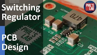
One thing that came in to my mind when using small resistors and capacitors like 0402. Keep the connected copper to them as unified as you can. We have had problems in the solder oven with components standing up towards the side with the largest copper connection. Several times I have had to decrease the conductor width towards groundplanes to avoid this.
Yes, tombstoning is the name of the phenomenon. Thermal relief on the pads becomes very necessary for these small passives.
@@wesleybecker834 is there a video that describes this topic in detail?
Amazing video Phil! Nealty explained to smallest details. Component viewer problem is going to be fixed. 🙂
Thank you very much! Love your services! :)
Enjoy the process being shown in a clear but detailed set of steps. Thanks!
Thank you for watching!
@@PhilsLab you specified the Dk value but not Df value, is Df not important?
Was waiting for the whole STM32 Altium schematic walkthrough :) Thanks Phil!
Thanks for watching!
The details and small practical tips in this video are really great! Not only for STM32 but anyone starting to work with microcontrollers.
Thank you, Tim!
Wow... This is your best video in my opinion this far... You explain everything.. I really appreciate that.
Thank you very much!
I have been using Altium from 99SE through all the versions and currently using 21.8.1. This is a fantastic tutorial and thank you. Maybe a few tutorials on some of the Altium features might be useful for some of the newer Altium users. (Library management, component creation (PCB and Schematic), DRC rules.
Please checkout the videos from Robert Feranec as well.
Amazing! Just staring out with Altium!love to see the whole design flow
Great to hear that, thank you, Rick!
@@PhilsLab at 3:20 you are talking about choosing the right microcontroller, are you considering this as a video subject? Would be awesome to het some insight in this.
PS do you have a PayPal so I can support you?
Great video! I want to learn how to properly do PCB layout and routing, I'm currently still learning EasyEDA and KiCad, but would like to try out Altium too!
If someone is wondering why sometimes you can't copy and paste MPN (Manufacturer Part Number) from JLCPCB altium, it because of the while spaces at the beginning of the MPN. You need to remove the white/blank spaces first. I am not sure this is clear but yeah, you need to remove the white space at the beginning.
Legend.
great video, can you please upload the libraries u used in this video on ur repo, it would be very helpful.
Wow! What a walkaround...... Keep up the good work brother........ All the best wishes for you....
Thank you very much!
Thanks for keeping it free
You're very welcome :)
great video i discovered 2 days ago and i watch many video most useful engineering youtube channel in youtube i hope cont keep continue !
You're such a nice teacher! Thank you so much for this king of video! 💞
Thank you very much for watching!
That's exactly what I asked for the last couple of videos !, Thanks a lot!
Thanks for watching!
Yessss, thats exactly what I was hoping to see from you. Thank you so much for your effort!
Awesome, thank you for watching :)
Incredible work as always. I hope someday in the near future the PCB design course :-)
Thank you! I'm currently working on the PCB design course, fingers crossed it can be completed in the near future :)
This was a great video, but I just had one question to clear up. The USB connector was not necessary and was just an accessory. From what I understood, we can just get +3.3 V power from the SWD header. Please correct me if I am mistaken.
thank you Phil , you're a blessing
Thank you for going into detail.
This is great intro to Altium. Thank you so much for your effort
Just what i needed, just got Altium
Awesome! :)
God bless you Phil. This is amazing
amazing content. well explained. couldnt ask for more.
Thank you!
Great job Phil ! I think the culprit for Altium not allowing to paste the part number is the space character at the end of the part number. Obviously it's a bug
I am grateful to you dear phil...I learned a lot from you..
Thank you, very glad to hear that!
Nice video. I hope You can design a esp32 board and give some design tips like in this video
interesting,how easy it is from you,and understending,but in my opinion wrey difiicult,tnx for all inserstanding tutotrials
Thanks for your videos Phil
Hi Phil, please show how to design low power PCBs for the STM32 chip. I feel many people don't know what considerations should be made designing one.
Hey Phil! Can you please share with us the libraries u r using.
I'll be grateful. Thanks.
Thank you for sharing such amazing content. Have followed recently and already got a lot of useful information!
Thank you for watching, glad to hear the videos have been helpful!
Fantastic walkthrough! Where can I find the schematic and footprints symbol library?
excellent tutorial ... !! Thank you!!
Thank you for watching!
Great video, one comment, keep GND names turned on. Sometimes when circuits are copied these names can change to something else, like GND1 or whatever the software decides to name them. If they are turned off you will not know that they have changed and may not be connected.
Great video, thanks so much for time and effort! I am just starting with Altium and this is a good reference!
Awesome, thank you for watching, John!
Excellent video.
Amazing. Software tutorials and programming would be also very helpful.
Thanks, Stefano - software and programming tutorials are already on my channel :)
Great walk through mate. Any chance you could do some tutorials on writing code and uploading it to the controller?
Thanks, Luke - I actually have some programming tutorials on my channel.
Love to see an usbc :) and an schematic with seperate usb voltage and external for a bit more current :)
where is the link that mentioned in 44:39 about ferrite bead?
thank you Phil your videos are very helpful
Phil is awesome engineer and kick as_ guitar free solo :)
Great work, i just want to know that +3V3 is connected through via and also GND, it look like the via are same and if though it should give violation for the short circuit because the +3v3 vias passing through four layers and as GND Vias. By the way Great work. Appreciations.
awesome video! I think you forgot to put your altium symbol and footprint library in the description. Can you please add them to one of your repos?
It's in this repository on his github -> AltiumDesigner-Libraries
Can you post a link to your library as you mentioned in the video. Thanks. Great video btw, better than anything else that is out there.
It's in this repository on his github -> AltiumDesigner-Libraries
Outstanding. Thanks.
Muy buen video, hace tiempo que quería ver todo el desarrollo de una placa con stm32!
Really great videos from you, already learnt to design myself and order from JLCPCB. Looking forward to next video. Are you planning the last part of Kalman filter? Best regards Martin
Thank you, Martin! Yes, EKF video is coming this month :)
Hello, good content and easy explanation, here you have provision of 4 layers, yet you used only top and bottom layer, you could have gone for just two layers
thank you a lot from Russia!
Thank you for watching!
That was a great tutorial, thank you very much. (I wanted to use the Altium lib that you uploaded on Git, it seems it does have all the footprints (just a limited numbers), but it has many more schematic symbols. So, maybe, would you please upload it again?)
Hi Phil - Excellent video. Can youb please remember to provide a pointer to altium footprint library. thanks
Absolutely awesome! So helpful!
Thank you, Mick!
2:23:10 What do you mean by "board warp", and why filling the whole top signal layer with let's say GND polygon is bad? I've always thought it's good for EMI protection.
Great video Phil! I didn't really understand where can this PCB design be used in. Can someone explain it to me? Thanks
Thanks so much for making all these tutorial videos that shows entire process from start to finish with the rationale for the decisions made. I have a couple questions about impedance controlled traces between your designs in the videos and in the GitHub repositories.
In the video you set up the USB trace widths for the JLC7628 stackup (0.26mm), but the gerbers in the GitHub appear to show them at 0.1532mm. Did you end up changing to producing this in the JLC3313 stackup after the video was finished? I'd like to get some boards produced and just wanted to make sure I have this correct.
I see a similar-ish thing with the previous LIttleBrain board, where in the GitHub history the USB trace widths were originally 0.2611 mm, but when you did a revision to remove the USBLC6-2SC6, the trace widths went to 0.2mm. Was that just a simplification and this level of detail doesn't matter at such short trace lengths?
Thanks again for all the fantastic videos.
hey , when i am updating the pcb document with schematic U2 is not coming ??
when i validate schematic there is it says no errors.
??
Talking about ferrite bead, isn't it that this component shall create large sharp peaks in the PDN impedance and thus is bad?
Great video. Your videos about pcb design assist to us. I have a question about stack up section. When you adjust the layers of the pcb, you selected in the power and ground layer as signal instead of plane. In this video you mentioned that this choices avoid creating a negative gerber. Does this choices make sense? The senior employees who work in our company always prefer the plane. I'm confused as a junior hardware engineer. Regards.
Thanks. I guess it's more of a preference/habit thing - there's no harm in using either.
This is one of the great AD tutorial on the YT. I could not found the library (symbol and footprint) in github page, could you pls tell us how to download it? Thank you a lot.
Could you find it? I had the same problem.
Can you help me find Footprint-Lib-PhilsLabPcbLib and Schematic... for me to be able to follow along
What about GND plane under the crystal oscillator? Great video by the way!
Great topic,, thanks 👍
Can we also add polygon pours for ground on the signal layers ?
Yo Phil, thank you for your video. Means a lot. Keep doing what you doing mate.
Hey Phil, awesome video! I think you forgot to put your altium symbol and footprint library in the description. Can you please add them to one of your repos?
Why connect the USB data lines if you're going to program using SWD?
Nice video, well done, thanks for sharing :)
Amazing video! and so forth :-)
Thanks! :)
excellent work. nice guide
Thanks for watching!
Are we sure that MCU has an internal crystal, not a lower precision RLC oscillator?
that is an amazing video to practice, thx to philip. I can't find the library. Can you help me to find it?
Thanks for great video. Where can I find the altium footprint library you used in this tutorial?
Isn't Altium still prohibitively expensive? Please correct me if I'm wrong
Pretty sure it is. What good is a free trial if you can't afford it after 30 days? But it's obvious why Altium would want to sponsor TH-camrs who've used KiCAD for many of the tutorials as it clearly cuts into their bottom line given the cost. Which starts "poisoning the well" of content most of us enjoyed before money hungry, corporate entities shut things down. I started watching this channel because of KiCAD...
Hi Phil, at 24:12, the first result is an oscillator, which correct me if I'm wrong but it needs just power and you have the clock output. Wouldn't be that more desirable than a crystal?
Where are the library files available? I can't seem to find it in the github repos.
I did not understand the topic whic was mantioned during 1:48:30. do we need pi filter even we have esp protection ?
Hi, you connected boot0 to ground because you said i will just be using swd. My question is; if we do that, can we program to our mcu via usb port?
You would have to write a custom USB bootloader to be able to reprogram the MCU. Otherwise, make a provision for pulling BOOT0 high.
Phil just a quick question, at the time of flashing code to the MCU, does it have to be done via an STlink or can it be done via the USB connector on the board?
Have you released the course you mentioned about a few videos back, I have been searching can't find a link :)
Why did you not seperate VREF+ (Called VDDA in KiCAD STM32 Video) to 2 different 3.3 Voltages, one Analog and one your common +3.3V?
Edit: I wonder if he ended up using a different STM32 board, and that is probably why.
great video also i was wandering the programing will be done via USB , right but cant it be also done with that header too ?
Brilliant 👏, thank you.
Thank you, Lee!
Can you do a modified version for 2 layers? Would be cool to see how you handle signal, ground and power on a 2 layer board.
It's 2 layer board?
For your personal projects, do you create your own symbol/footprint before starting the schematic design or settle on what the manufacturer part search offers?
Why do you need two ground planes. Why not only 1? I think that you don't even use L3(GND) plane since all the ground connections from L1 go to L2(GND).
Are all the I/O pins of STM32 active low?????
can you provide some link to recommended library?
After placing stitching vias, do you need to repour your L2 L3 GND copper polygon?
In the PCB stack, you entered the value for Dk but not Df. Why is that?
Thanks for this great tutorial! Really useful!
Are your custom libraries already upladed? I cannot find them
Thanks Phil! One question - if you have two or more crystals on your PCB of different frequencies, do you need to keep them far apart?
is double sided pcb where bottom is digital and top is analog good idea? 4 layers, top 12v, bottom 5v and 3.3v and middle layers both ground?