Metallization: Making Conductive Traces on Silicon Chips.

ฝัง
- เผยแพร่เมื่อ 29 พ.ย. 2023
- Support me on Patreon: / projectsinflight
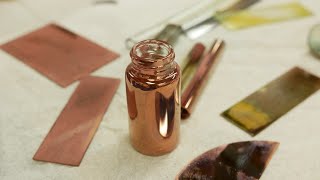
In this video I attempt several methods for applying metal layers on silicon chips in order to find a hobbyist-friendly way of making conductive traces on silicon.
DISCLAIMER: The videos on this channel feature materials, equipment, and activities that may be hazardous. By choosing to replicate or participate in any demonstrated activities, you acknowledge and assume all associated risks. You the viewer are responsible for your own safety. ProjectsInFlight and its creators are not liable for any resulting harm or damages. - วิทยาศาสตร์และเทคโนโลยี


Actual technical aspects aside, I was much more impressed and entertained by the critical thinking and problem solving involved in this one. It's very satisfying to see you go through all the stages of hypothesis, experimentation and adaptation
The allure of cheap materials is their cost, but the low cost always comes with terrible side effects. You need a proper magnetron if you're gonna do this. Trying to do it without one is like a carpenter that doesn't own a hammer. And if you've got a magnetron, you have a plasma cleaner if you just fill it with oxygen and light it with RF. You can't make chips without a variety of vacuum systems. They're as essential as the furnace. Don't misunderstand, your efforts thus far are awesome. But you're going to hit a wall really really fast IMHO. Keep going, looking forward to seeing how far you make it through this.
not to spoil and upcoming video too hard but... i already built my thermal evaporator
@@projectsinflight please tell me it's made out of components from a regular microwave
@@janthran For coating metals using PVD the more expensive parts are the pumps for the vacuum. The graphite boat, a high current transformer or inductive coil are relative cheap
Like your stuff @thethoughtemporium, but I disagree with you here, as is, disagree with telling people 'can't do X because..' especially when they are making very impressive headway doing X.
Although usually you are right (and as the replies show, you are) you never know what cool things come from smart people delving into projects they know nothing about, since they don't know you can't, and on the rare occasion, they end up showing you that you can.
@@evilplaguedoctor5158 Agreed. Honestly feels like a pretty out-of-character comment from thethoughtemporium, but I guess now that they've got a big honking lab and apparently plenty resources, only the grandest of plans are worth the effort, or something. Idk, you put it pretty eloquently, but there's also something more in their comment that rubs me the wrong way.
I think you can avoid the problem of silver coalescing into small blobs by first alloying the deposited silver with a bit of copper.
You can deposit some copper very quickly (you don't need much) with a copper sulphate solution and a DC voltage. As soon as you have some deposition, take it out and bake the chip. Over time, the silver and copper will alloy into each other (fairly quickly as well, since copper in particular is amazing at solid state diffusion), and you'll end up with a layer of some grade of sterling silver instead of pure silver.
The sterling silver should allow you to anneal it without it coalescing into blobs and losing all electrical continuity.
this is a really good idea and i'm gonna test it as soon as i can
every time you upload I get excited to see how much progress you've made, can't wait until the day you make your first chip, even if it's something as simple as an And-Gate or something else.
probably a differential pair i think
As someone who has coated telescope mirrors with precipitated silver, once you finish them, they are never touched with anything other than running water.
I'm commenting before I finish watching the video just because. I make soap and I can very much attest that dissolving NaOH in water produces a *lot* of heat and can even boil the water if you add it too quickly. The "go slow and be careful" is very good advice for anyone not familiar with it.
finnaly
i wasted 2 years of my life trying to do exactly this, never finished.
thank you
Thermal evaporation wasn't really used in IC fabrication past the 70's to early 80's, as it isn't really that much cheaper or easier than magnetron sputtering, but it does have many unique disadvantages.
If you do intend on acquiring dedicated equipment for metal thin film deposition, I would *strongly* suggest going with a magnetron sputtering setup, even when choosing between a DIY bell-jar-based magnetron system and a commercial thermal evaporator.
As for the current process, getting an adherent film on a homogeneous, smooth and flat SiO2 surface is great and all, but I fear insurmountable issues lay ahead if you try to use this process to contact exposed silicon through holes in the SiO2 insulation.
8:45 never underestimate the strength of silver fulminate, even small amounts you can barely see
yeah i've heard stories of high school chemistry teachers accidentally blowing up their storage closets after this demo
@@projectsinflight imagine trying to explain that one to the school administrators
One thing you could try is electroless copper plating, the process they use to create the initial copper layer in plated throughholes in PCBs (in PCB manufacture they then build up that layer to final thickness through electroplating). It's reasonably quick (from what I can find about 15-20 minutes for a 1 micron layer), works on glass, and DIY-kits for it are available online (although not necessarily cheap).
i'm not familiar with an electroless plating solution that works on non-metal base layers
@@projectsinflight есть статьи на нескольких русских сайтах - там радиолюбители, используя практически кухонную химию (кроме гипофосфита кальция - его покупают в интернет-магазине или магазине радиотоваров), получают первичную металлизацию (в их случае - металлизацию отверстий в стеклотекстолите). Если интересно, я могу отправить Вам на почту ссылки на эти статьи
@@projectsinflight Well, the inside of your glass bottles seemed to work.
@@projectsinflight Electroless plating is an autocatalytic chemical deposition process specifically for non-conductive surfaces, used for example to metallize plastic surfaces or as I wrote plate the insides of vias/through-holes in PCBs. It actually works somewhat similar to your silver mirror process, except that a catalyst is attached to the surface first (in a so called activation step) so that the chemical reaction that produces the plating metal only happens at the surface that you want to plate instead of in the entire plating solution. Wikipedia has an article about the fundamentals of the process, just look up "electroless deposition".
Maybe you're confusing it with electroplating?
@@projectsinflighti was wondering if you could start with a silver layer like this and then use electrolysis to make it stronger and adhere better, maybe using the tube furnace to either get the silver to ball up and let the copper or aluminum or other metal have better access to the silicon (after you make enough of a layer for electrolysis to keep working) or maybe even melt it enough to to form an alloy of copper and silver
Just an idea but check out plating plastic with metals videos. Now that you have basic conductive layer using the mirror method, you could use some light electroplating to increase durability significantly on your deposited layer. This would likely create a thicker more continuous layer without require anything to major in material or equipment. The electroplating rub on method that is often used with gold plating and other expensive metals should allow relatively controlled deposited layer that is actually adhered to itself and should be relatively quick and easy to do. I hope this is helpful in improving you design. Can't wait to see what your next version is like, awesome work
This is the kind of amazing content that is so often sorely missing from this site! Thank you so much for the highly detailed info
This made my Thursday. Thank you! It's very motivating to see you persevere through all of the challenges of this project.
Honestly I have just been living this series.im excited to see what your next project so going to be once you finish this one
Loving these videos and your progress, also a huge thank you for sharing the issues you faced and how you solve them rather than skipping straight to the "here's one i prepared earlier" style.
This is such an awesome project, can't wait to see more!
This is my favorite Project on TH-cam right now.
Thank you so much for your amazing work ❤❤
Very cool, step by step finding a way. As always a pleasure to watch, thx for sharing.
Loving the progress in these videos!
BABE! WAKE UP! NEW PROJECTS IN FLIGHT VIDEO JUST DROPPED!!
Man, I look forward to your videos! I'm so invested in seeing you succeed ;)
It's fascinating to watch you solve problem after problem with improvisation, this is a great series. It looks like the acetic acid is working well, but if you're so inclined, you can make a "poor man's" nitric acid by mixing sulfuric acid and potassium or sodium nitrate. Potassium nitrate is commonly available as Spectracide "stump killer."
Amazing video! What a showing of skill and determination
I am having one of those very rare events where the algorithm truly picks something and someone worthy to introduce. Great info, amazing work, subbed right away. Thank you for the hardwork.
I really like your style of narration.
good work!
This is what engineering is about! Though I do suspect that you'll end up having trouble down the line with using silver. So probably better to slowly start working on that thermal evaporator or sputtering magnetron sooner rather than later :P
already on it :) i got a turbo pump off ebay
This is awesome. You are quickly becoming my favorite channel.
For the home lab a tiny vacuum chamber should be plenty and I think if we could make a few custom Mason jar lids with a vacuum adapter and various tools it should allow anyone to do thermal deposition, CVD, PVD, and ALD for under a few hundred $. It would be big enough to fit 2" wafers and old DLP projector optics allow projection lithography to be done very cheaply.
well done, enjoyed the whole process!
Fascinating!
Very impressive!
Wow! This is amazing progress. I really want to see you make a functional chip. Maybe something simple like a few not gates, or other 7400 logic. I can imagine a future where instead of making just printed PCBs, maker spaces might be building their own self contained ASIC fabs for their projects. This is freaking amazing!!
Edit: p.s. This is the first channel I've ever hit the little bell on. I don't want to miss an update!!
i suspect a differential pair will be my first IC
@@projectsinflight complete with current mirror?
So enthused to see another video up
amazing work.
Hell yea, finally. Love the series
As a previous commenter noted, the critical thinking and problem solving are very interesting/entertaining but I also enjoy your speaking style, your clear enunciation and intonation. Thanks for sharing your work; I know it takes a lot of effort to research, plan, execute and record, then edit and post these videos. Very nice!
❤ for your dedication
Fantastic! Thank you very much for another incredible video.
I could never be patient and methodical like that. I'd probably lose my mind way before this point.
wow congrats! what a journey
thanks for sharing.
very cool! It might be interesting to try electroless copper plating on the silver traces to increase their robustness instead of the copper paint
Honestly I’m amazed you can get Riston to stick to a polished wafer, that is no easy task! In the past I’ve used spray-on negative pcb resists on silicon wafers with good adhesion but they can be a pain to remove, required warm baths of 2M hydroxide. Good luck with the evaporator, in my experience, it’s cheaper and faster to use coiled tungsten baskets as opposed to boats. The boats require 100s of amps whereas a tungsten basket gets just as hot with maybe 50-60amps. They work really well for evaporating chromium because it doesn’t melt it just sublimes at the right temperature, if ur using gold or aluminum then sometimes the boats are your only option. Also as a hobbyist I would definitely shy away from the expensive deposition monitors and just use a dremel to break open a 1-10Mhz crystal oscillator and use a USB oscilloscope to measure the changing in frequency with a small bjt driven amplifier.
hey, you seem like you've got a lot of knowledge on the subject. if you want to connect feel free to email me at projectsinflight at gmail dot com and i'd love to talk if you have time :)
I've been following you for a few months - Excellent approach and progress. Consider UV Resin as a hard/permanent protective coating!
Absolute legend right there.
Dude keep these coming so good !!!!!!!!
Thank you for share your efforts and experiences. Pleas make a video on transistor making at home by common available chemicals.
This is some methodical and metriculous work that brought you to this success, well done and congratulations!
Back in the day, we used to selectively create small silver particles directly where it was exposed to light, without extra photo resist (a.k.a. common silver photography). I am wondering if such process could create a useful conductive layer, though I suspect that the particles will be far apart and not connected.
congrats man :D I would love to have one of your throw-away failed little Si chiplets, would be neat to have a little piece of what may become *eventually* the go-to method for home labs making their own custom integrated circuits... you could be onto something huge - and all the very best to you my man! :D
Like always a great video. I have to try this at some point.
keep me posted:)
Very cool!
Wow. You are good chemist.
Would be neat to see a working circuit using this method. So neat and way cleaner then most chip manufacturing processes. If you give it a coat of UV Epoxy that would effectively make it a durable product that is also quick to apply. Love this.
Dude... This is awesome
Forgot to mention this to anyone testing electroplating the mirror finish deposit on silicon, would likely require the use of alternative electroplating solution as the ph of tradition electroplating solution would likely be too acid. A simple alternative could be using DES, deep eutectic solvent, which is essential mixing two solid chemicals that make a liquid chemical. Often this process can be done with just mixing the chemical together, might require mild heating. The ph of is often closer to neutral than water based plating solutions. There are a large variety of DES that could be used for this but I would want to use something biodegradable like choline chloride with ethylene glycol, choline chloride with urea or even just urea or choline with metal salt that is deposited, ie silver chloride. DES can be formed using metal halogens as being one of the chemicals. Good luck to anyone trying.
I've been wondering about silver for hobby IC labs for a while, great to see it in a video. A future problem you might run into with silver interconnect is electromobility; low melting point metals tend to have atoms pushed out of place over time by electrons colliding with them as current flows, altering electrical characteristics, I think it's just a problem with smaller wires though, as aluminum interconnect is widely used in the thicker global interconnect layers and also has a low melting point.
Great work. You are getting close to make your first semiconductor device😊
next video should be diffusion. very excited
Absolutely amazing! I was already considering trying to figure out my own ways of doing these things without a giant lab like Sam Zeelof, and (if i ever do try anything like this lol) this is amazing information, especially since I am quite useless at chemistry...
WOW. Just WOW I'm amazed with how much you are accomplishing. God I love living in the future!
That's awesome!
Awesome video !!!
Very cool! Cheers...
As someone has already suggested, I would try to electroplate the silver layer with copper and then bake it as you did. Copper layer might prevent silver from beading, and it might adhere better to the silicone(oxide) substrate. You should be able to make the plated layer even thicker then original silver layer, so conductivity will be better too. Might not work with just silver on silver layer, but you can give it a try. Electroplating should be relatively easy and you can try different metals too, but I believe copper is the easiest to achieve and could work well with silver and heat.
Very cool, keep it going
To solve the silver beading problem try annealing the layer with an additional Si or glass chip laying flat on top of the target chip. The surface tension should spread out the Ag layer (the method has been used for growing thin films of metallic single crystals from metallic solutions)
Hey, you seem to know your stuff. if you ever want to chat my email is projectsinflight at gmail dot com.
Genius!
Thanks!
In commercial mirror making, I think they use wet deposition of tin or chromium as an adhesion layer, or occasionally some metal oxides. Tin (II) Chloride mixed with HCl, if I remember right, but it's annoyingly hard to find any open access articles for it right now. I kinda suspect it will be really hard to avoid using vacuum processes for silver deposition of high enough quality and adhesion for this use case though.
I really liked your conductive paint, so I looked up online, yes! There is a thing called doped silicon ink. You can just "print your own transistor" with doped silicon on paper(?) with a suitable printer.
oh, interesting! feel free to email me the link. my email is projectsinflight at gmail dot com.
Love all your effort and I am trying to guess how to keep the silver layer stable for the moment the semiconductor heats up.
the semiconductor substrate shouldn't need to be heated for any fabrication step after the metal is added, and devices shouldn't operate at temperatures above about 200C
OK so rather than a plasma cleaner, UV ozone is a good final cleaning step and dead simple. It will make things more reproducible. Just get a UV lamp with the right envelope so the 185 nm light gets through and produces ozone. Expose the surface to be cleaned to the output of the UV lamp at relatively close range. At ambient temperatures it trivially eats few-nm layers of organics and makes everything pass the water break test with flying colors every time, the water just zips across the surface at first contact, so it's good after wet cleaning. If the surface is heated, you can even eat through um thick layers of organics.
Logistical issues: run the lamp in an enclosure, but UV ozone will slowly erode anything organic. A simple setup is to have the electrodes outside of an enclosure, and the silica envelope of the lamp goes through the enclosure. Watch out for some supposedly single ended lamps that aren't really single ended, they just have a PTFE coated wire going to the other end. Also disposing of the ozone can be a pain, but it is decomposed by 254 nm light, so if you get a second non-ozone-producing lamp you can use that to destroy ozone. Putting the setup near a fume extracting device is a good idea regardless.
This may be a bit much, but it's a lot cheaper and easier than a plasma cleaner and gives as good or better results for many applications.
Would a normal o3 generator work to clean things? Assuming comparable safety measures.
@@nocturnhabeo Not nearly as well--less effective than 254 nm UV alone. The ozone isn't actually the most active part. The UV lamp produces 185 nm and 254 nm light, which produce and decompose ozone respectively, and in the process produce atomic oxygen. The UV light is itself absorbed by organics, which causes additional reactions rendering them more reactive to oxidizing agents. An ozone generator and 254 nm UV light might be similarly effective with the right parameters.
OK I did a quick search on google scholar. It looks like the 185 nm UV is probably doing most of the work, both in forming atomic O from air and in directly attacking chemical bonds. The 254 nm UV is largely irrelevant or mildly counterproductive, but mercury vapor lamps are cheap so still probably the thing to use.
this is very interesting- thank you for the detailed write up
Maybe spray-on photoresist like Positiv 20 could be used to avoid fiddling with the teflon tape. And maybe some thin layer of electroplated copper could improve the durability and conductivity of the silver. It won't improve adhesion though. Pre-etching the SiO2 layer a little bit might help with that by modifying the surface.
sadly i cannot find positiv 20
I was a little sad to see the beaker die an energetic death, but then I realized if it's that easy then it's easy enough for me to try.
You are insane :) insanely good
You could try to plate the silver layer with copper or another plating compound
I would love to see some cross sections of these prints. Might be able to use a SEM at a college in the area if they have a material science course. Other than the sticking issue, I am really curious if silver has the same "creep" problems that copper does. Copper likes to create all sorts of wild hairs that short circuits out in semiconductors.
sick
Mr Projects, would you like an ACIDIC SILVERING process i stumbled upon? Maybe it won't destroy your photoresist and you could try the lift-off method. You need your silver nitrate, citric acid, disodium EDTA and ascorbic acid, yes, vitamin C. Parts are sensitised with SnCl2 and AgNO3. I've used it to plate things like flowers, plastic dice, and glass of course. You can ask here for deets.
You can also check out Brashear's method for silvering telescope mirrors for the SnCl2 thing and other ideas in general, they end up with thicker layers that can be polished using the alkaline silver method.
Very impressive! At this point would you consider vacuum deposition again?
I think with silver you're going to run into issues pretty fast as you try to make more complex designs and add more processes onto it. There's some thermal evaporator build series on TH-cam that could give you a good starting point.
not to spoil an upcoming video too hard but... i already built a thermal evaporator
i wonder if pasive electroplating could improve the sructural strength of the base metal , there are cold tining solutions avalable for normal electronics but it is ostly ment for copper
but if it work it could stick together loose silver bits into single metal foil made out of tin and silver. i am not sure if it would stick to silicon by itself and even aplied to silver it would still relay mostly on silver to silicon bonds
This is really cool! I was wondering whether it would be possible to use the initial silver plating to then use electroplating for a thicker layer of e.g. copper that would survive the annealing process and better adhere to the silicon surface?
i'm definitely gonna try this if i can. this is a very good idea
When you first started talking about a chemical process for depositing silver, I was sure you were going to go with a photographic process, like tintype or daguerreotype. Both produce silver images on glass and would skip the need for photoresist, as you could just expose the traces directly.
(I'm not sure if gelatin is left behind in the process, or if the silver crystals are touching or not.)
i'm not an expert but it seemed like the daguerreotype process needed a silver layer as it's starting point, so i'm not sure if it would make anything easier. i could be wrong though
18:40 Nice, you made flexible electronics.
hahaha maybe i should explore that
It's not the nitric acid that allows dissolving silver metal but rather the nitrate ion. You can actually add a small amount of potassium nitrate to another acid and it should work just as well as aqua regia. Don't remember where I saw this, but it was another chem youtuber
17:31 I thought you were gonna say..sometimes the best solution..is found in the kitchen
Bro, your glucose concentration is actually 9.09% not 10% not sure if 1% would trow off your results. Thank you for sharing this video it really inspires me to get back in the lab.
yeah sorry that was an oversight. fortunately the reaction is not too sensitive to glucose concentration
this is a weird combination between surprisingly simple and complex. Stradling the line between, I could do this and I really don't want to do this
Are you sure that a thermal evaporation would have been too costly/too much hassle considering what you had to go through?
A very basic setup consists of:
- a molybdenum/tungsten boat (an embossed strip)
- thick steel rods for electrically contacting the boat
- high current power supply
- wire frame to hold the chip
- a vacuum chamber
- a vacuum pump
Four of these things you can buy cheap-ish. The boats are like 5 eur per piece, steel rods and steel wire are cheap and a 12 v/40 A power supply is also cheap. You don't need an extremely high vaccuum, so a cheap-ish pump will do and you don't need a large chamber at all for coating small chips. A cup-sized chamber will do which also reduces the cost a lot. The trickiest part would be making the vaccuum chamber that has isolated feed thrus for the contact rods (at least one has to be isolated from the chamber walls, the other contact could be ground and be fixed to bottom plate of the chamber). You made a tube furnace, so this should be well within your reach, tho.
i don't want to spoil future videos too much but... i already built my thermal evaporator ;)
@@projectsinflight
Amazing, dude. I signed up as patron because I really want to see you succeed with this.
i don't want to spoil future videos too much but... i have already built my thermal evaporator. i do really appreciate the thorough feedback though :)
Can you use sputtering for depositing a thin layer of metal?
What about quickly dipping the wafer in molten aluminum and then etch away the excess thickness with HCL or HCL-H2O2 until reach a desire thickness?
Another Idea would be to laminate the wafer with aluminum foil and the put in the furnace for sometime until melts.
8:23 "It just works"
-Skyrim man
Hi man, weren't you able to finish the semiconductor device? I was expecting the remaining part of the process I think you do an amazing job here, best regards!
oh, that video is coming don't worry
WOW!! that really was A LOT of near dead ends, but you over came them all!!! SWEET!!!!
about making a chemical vapor deposition apparatus, I know that the AMAZING channel 'Applied Science' made one on his channel, AND he also did a lot of the stuff you're doing... sooo I HIGHLY RECOMMEND you check out his channel and pull some knowledge from his experience to apply to your own process (I'm not saying repeat what he already did.. what's the fun in that? .... but there might be some things he might have already shown that could help you avoid dead ends that are costly in time and money.... ESPECIALLY with the CVD chamber.... Hopefully it's helpful)
oh yeah Ben is great- i'm definitely interested in building an electron beam like he did but for lithography
What about taking advantage of the conductivity of the poorly sticking silver layer just as a precursor for electroplating? If you have all of the traces temporarily shorted together in the design you could nickel electroplate over the silver for example. You could keep building it up to a fairly robust layer. Hand Tool Rescue uses the method to nickel coat steel tool handles. I have no personal experience or data, it just popped into my head. I also wonder if you could attach super thin metal foil in one corner before you silver plate so that you have a pad to contact electrodes to.
this is a good idea and i really need to test it. it might make it possible to anneal the layer without it beading up
@@projectsinflight I was also brainstorming and wondering if you can leave a permanent resist layer with silk screen printing instead of using PCB photoresist. The ink is pretty rubbery and thick so I am wondering if you can mechanically sand off the conductive layer off the mask after without trying to use solvents.
@@projectsinflight I have plated nickel, through great pain. Two things about it: first, nickel is hard, like harder than most steels. It will never scratch off if properly plated. Use this to your advantage and beware of plating things you don’t want to plate - it takes a long time to take it away TuT. Second, it is very hard to plate in DC currents without using a fancy commercial electrolyte. You definitely can. If you attempt it, the key parameter you want to control is the current density. Godspeed. 🫡
Would it be possible to use the silver anneal beading effect to create patterned discontinuities?
maybe, but the beading effect is on a very small scale and i'm not sure what i'd be able to do with it
Pretty sick you reach this point with your equipment, it's a wonderful step up for the process, not perfect but is insane you can go this far.
@21:18 - My thinking is to take a thin sheet of PEI like I use for 3D printing beds and sandwich the chip between those for the lamination? Heck, even an iron won't melt PEI. I way out of my element here though.
I just used Ferric chloride to etch silver coating 😊
Do you think if you physically etched the chip face would the deposited silver be adhered better... using either ceramic, carbide, garnet, or even cut glass as a media? I have a small glass etching "airbrush" made by PASCHE which can do small fine work at lower pressures.
etching the surface would likely help adhesion, but it's likely that would damage any devices that exist on the silicon at that point.
@@projectsinflight my mistake I thought prior to coating there was nothing on the silicon. I thought it was blank.
How do you make such good mask?
You could do tests with other metals. I know you can do copper with that one blue crystal. Copper sulfide? Idk.
As for cleaning, is there a reason a laser engraver or cleaner wouldnt work?
And what materials could you deposit to make transistors?
depositing copper mirrors instead of silver requires a stronger reducing agent than glucose, usually hydrazine which is toxic and flammable.