Should you place solder mask over BGA pads? Do you know why? | Tom Hausherr |

ฝัง
- เผยแพร่เมื่อ 29 ก.ย. 2024
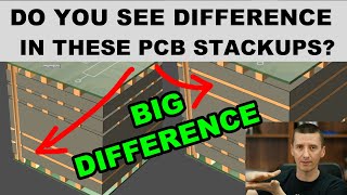
- How to decide on BGA pad size and if SMD (solder mask defined) or NSMD (non-solder mask defined) pad should be used. I asked Tom Hausherr
You can watch the full interview with Tom here:
• How to create perfect ...
Links:
Tom Hausherr: / tom-hausherr-cid-cit-4...
Tom's company website: PCB Libraries www.pcblibrari...
------------------------------------------------------
Would you like to support me? It's simple:
Sign up for my Hardware design and PCB Layout online courses: academy.fedeve...
You can also support me through Patreon: / robertferanec
Or sign up for my Udemy course: www.udemy.com/...
It is much appreciated. Thank you,
Robert


![CAMPปลิ้น | EP.82[1/2] แก๊ง 3 สาวเพื่อนซี้บุก CAMPปลิ้นครั้งนี้ห้ามเสียอาการ](http://i.ytimg.com/vi/_6WUjXHe1TM/mqdefault.jpg)

I'm just loving these shorter snippets of useful information! As much as I like the long interviews, it demands some commitment to sit down and absorb it, bite-sized videos are more compelling.
I believe you can specify a negative solder mask expansion on pads etc to achieve that effect. I do that on vias for "tenting" (not true tenting probably but covers majority of the via annular ring)
Simple solution to the pads ripping off: everyone should go back to only using through-hole components! 😂 Just kidding
Maybe a “star” pattern on the pads so there are holddowns around the pad but the solder can get around the pad in 6-8 spots around the pad. Combine both approaches.
So what happens if you put solder mask the same way as thermal reliefs so not a complete ring but a couple of edges. I guess a straight line like a thermal relief is not a good way but maybe like half circles. That way it kind of looks like a flower pattern from the top. Would the ball be able to collapse partially onto a pad and the parts of solder mask that stick over be able to hold the pad better.
Oooh, I wrote the same thing! Great minds think alike.
great info!
Would you also find the same problems with other SMD components with the copper pads ripping off during drop tests/vibe?
I think its harder for other pads since they are generally larger than those tiny BGA pads. Larger pads means more "hugging" to the Epoxy I'd think. Fair warning though, I have never done any vibrational testing but I do PCB design too, simpler stuff.
Very clarifying, thank you Robert!
Really appreciate these shorter clips, very informative.