Hey, thank you so much for uploading such an informative material for the students. Could you please upload a vedio which contains all the info about PCB like what is PCB, it's types, it's raw material, it's process. Also how do we calculate the cost of PCB. I'll highly greatful to NEWBURY ELECTRONICS. Regards. Kamya Luthra
I have watched just about every PCB video in you-tube and i have to say this one is one of the best,nice videos on here well done! Also the work environment look very nice and i bet its nice to work there!
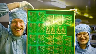
Some questions: 1) What is the typical level of radiation left from X-ray process on the boards after production and how is it kept safe to limit exposure to staff who constantly produce these products? 2) What happens to the activated carbon that cleans out the heavy metals from the water? 3) the result of the strip-etch-strip line looks like pure art to me, do you ever have "mistake boards" at this stage in production that you'd be willing to sell? I think it would look fantastic with a frame around it.
Hi Jonathan, Thanks for your comment. 1) The residual level after production is “background” radiation. No additional radiation lingers in the product. The equipment is checked annually for safety when external radiation leakage is checked and certified safe according to legislative requirements. The X-ray equipment is manufactured in the UK by a respected supplier. 2) The carbon is removed under hazardous waste legislation, and incinerated off-site to produce electricity. All waste transfers are documented. 3) We have some scrap at this stage, although only small amounts. All scrap is recycled to recover the copper content, so I regret that we don’t normally have spare pieces available. However if you leave contact details with us, we can send you some scrap sheets. Any other questions, please let us know :) Newbury Electronics


Im an electric engineer . and i really wanna say . this video was great and useful . thanks alot ..
We're very happy to hear that an electric engineer found this useful. No problem.
Hey, thank you so much for uploading such an informative material for the students. Could you please upload a vedio which contains all the info about PCB like what is PCB, it's types, it's raw material, it's process. Also how do we calculate the cost of PCB. I'll highly greatful to NEWBURY ELECTRONICS.
Regards.
Kamya Luthra
How does the carbon hole metalisation compare with the electroless copper deposition? Is there any difference in performance/ cost?
Excellent video! Thank you for creating and posting!
Great Video and good explanation... Thank you...
I have watched just about every PCB video in you-tube and i have to say this one is one of the best,nice videos on here well done! Also the work environment look very nice and i bet its nice to work there!
Glad to hear that you enjoyed it :)
Some questions: 1) What is the typical level of radiation left from X-ray process on the boards after production and how is it kept safe to limit exposure to staff who constantly produce these products? 2) What happens to the activated carbon that cleans out the heavy metals from the water? 3) the result of the strip-etch-strip line looks like pure art to me, do you ever have "mistake boards" at this stage in production that you'd be willing to sell? I think it would look fantastic with a frame around it.
Hi Jonathan,
Thanks for your comment.
1) The residual level after production is “background” radiation. No additional radiation lingers in the product. The equipment is checked annually for safety when external radiation leakage is checked and certified safe according to legislative requirements. The X-ray equipment is manufactured in the UK by a respected supplier.
2) The carbon is removed under hazardous waste legislation, and incinerated off-site to produce electricity. All waste transfers are documented.
3) We have some scrap at this stage, although only small amounts. All scrap is recycled to recover the copper content, so I regret that we don’t normally have spare pieces available. However if you leave contact details with us, we can send you some scrap sheets.
Any other questions, please let us know :)
Newbury Electronics
我的天啊真的好落后的设备和技术以及产品了。
Nice video, thanks :)
Impressive
At the beginning, I thought my Display has gone crazy... :D
Nice view of the process. As you would know China has taken the business certainly in the hobby or maker market.
Passions
После JLCPCB это не современная фабрика, а совковый колхоз!