#1226

ฝัง
- เผยแพร่เมื่อ 15 ส.ค. 2022
- Episode 1226
I give KiCAD a try. Seems OK, not a fast user interface but gets the job done. I've been limited to small boards due to Eagle limitations. Now I can do larger boards and multilayer!
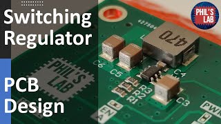
I've taken all the synth circuits and put them on one board.
the following is a rev C of the board, but decided to link it now if people are interested
get PCB: www.pcbway.com/project/sharep...
Be a Patron: / imsaiguy - วิทยาศาสตร์และเทคโนโลยี


![CAMPปลิ้น | EP.77[1/2] ก็ไม่ได้ชอบเอาชนะ แต่เรื่องอะไรต้องแพ้!!](http://i.ytimg.com/vi/JraaBYOd7I0/mqdefault.jpg)


I am sure you know that Q5 as a voltage shifter has to go to the input of a current mirror at -12V which goes with its output to R21. (adding 2 transistors (and maybe one resistor))
I also use Kicad. If it doesn’t have a part or symbol I like, I go to mouser and find the part. Then I use their library loader feature to import the symbols into kicad. Really helpful way to get symbols and 3D models for parts I want to use. 73
neat project, good work.
Now I wanna try Ki Cad.
Eagle was acquired by Autodesk and they are embedding the schematic/PCB design into Fusion which is free for personal use. I don't think it has limtiations in terms of board size. I'm working on the first project and will start the PCB design soon so I'll know ;)
But KiCad is very good too.
You *can* add the mounting holes to the PCB only. You only have to be careful if you then make changes to the schematic and then pull in the changes to the PCB - you have to make sure to check (or uncheck?) a box that indicates whether to blow away existing components on the PCB in order to retain them.
it'd be nice if that was a component level feature instead of an overall preference thing... is it?
use version 7, design the board, place the components on the correct spot and switch to 9 to route, no limitations.
the dumb part of kicad is binding a footprint to a symbol.
it's the same in eagle of you wanna have them grounded, unless you place simple holes with the stop layers.
3:31 You can use a FET (2Sk30A, BF256, 2n5485, etc) instead of R40, R41, C5, like Roland did in the Jupiter 8.
this last transistor of the CA3046 (pin 12, 13, 14) has usually all pins tied to a negative voltage divider, -1V, substrate, all designers in the past did this.
check the "schematic" of Doepfer A110 VCO.
There are two additions I heartly recommend. The first ia an autorouter. A bit of hoop jumping to install it, but it works great. I tried it on a board I was trying to route with no vias. It did it and most of the board looked like my routing. The second is a melting plugin. It takes your cold hard edge traxes and makes them curvey. Fat tracks and spacing (1 mm) makes it look almost hand laid with vinyl tape. Mitxela has a video on melting and Sukesh Rao M has the deets on the autorouter.
I tried the external autorouter. I found it very slow and difficult. I'm used to a build it router where I can autoroute only selected lines and not then entire board. Auto routing section by section can get very good in digital designs, say just autoroute the address and data lines first.
in Eagle you have the Mitter tool in the toolbar on the left, select or introduce a radius and click dimension layer on the right, 2 types available, job done.
It's best to hand route, the top layer form west to east or vice versa and bottom layer from north to south, use the component pads to switch layer and if no options available use 2 or 3 vias.
i lay my tracks with the calculator, (1,27, 0.635 ) and route them exactly between pins of ic's and components, than i use the mitter tool to round them off in the corners.
This is a great project! Thanks.
thanks. just to let you know, I gave your old radio to a friend and got him back on the air
@@IMSAIGuy That's great news! I'm glad someone's enjoying it.
Nice project - good documentation 🙂
Glad you like it!
Interesting stuff, thanks for the cool opamp projects. I've been designing some eurorack synth modules in kicad for a while now. The real question though... Why the European resistor symbol and the American potentiometer symbol??))
Yeah it has been great fun !....cheers.
Yes, so far, so fun!
For your first custom symbol, you did a good job on that CA3046. Multi-part symbols can be a little tricky. Do you explain in a previous video why you needed to use that particular chip rather than a few more 2N3904s?
You certainly can drop in mechanical components like mounting holes directly in pcbnew. Just remember that, if you need to update the netlist after modifying your schematic, you might have to put the mounting holes back in afterward and reassign them to the ground net. It's more convenient to just put them in the schematic. If they're purely mechanical holes (not connected to any net) you can make them edge cuts on the mechanical layer, but a fabricator might have trouble interpreting them as holes.
Actually, you can build an entire circuit in pcbnew in standalone mode, but you won't be able to do any DRC. It's convenient for simple things like Big Clive's Disko Shart boards.
yes, it was explained, the long tail pair needs to have matched transistors. the bottom pair and top pair of the filter the most important
nexperia sells matched transistor pairs pmp4201 iirc - i think that’s what moog used in the werkstatt.
I saw those, super tiny
Nice PCB layout.
Instead of the jumpers for the OSC/NOISE/SQ to MIX, you could use DIP Switches. :)
thought of that. this allow non-standard jumping
A reply to AnalogDude, & IMSAI Guy: . I rarely let an entire board be autorouted, Important or special tracks first then auto if the board is large & complex. Or I'm being lazy. Or it really simple and I'm lazy. I most times prefer the no via version because I etch (now trying routing) them myself and vias get forgotten about. TH (no P) parts are my vias 😃. As for curves plugin, its easy to use and really shines when making boards from old magazines. Creative options are always welcome and if not, ignore them.
If I could ask, how soon after you submit gerbers to PCBway do you get your boards delivered in your experience?
depends on what shipping option you choose. But about 1 week for me
@@IMSAIGuy Thank you! I have a protomat and typically mill my boards, but as they get more complicated, I need to send them out, particularly 4 layer boards, and needed hi reliability two layer boards.