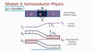
Forward biasing and reverse biasing of p-n junction diode on the basis of energy band diagram

ฝัง
- เผยแพร่เมื่อ 7 ต.ค. 2024
- Forward bias and reverse bias characteristics of p-n junction diode are explained on the basis of Energy band diagram in this video.
Sound credit : Chaitanya


This is the best explanation on TH-cam about this topic 👍😊
Thank you for the complement🙏
great video sir, thank's a lot
Thank U so much Sir for your Wonderful explanation 🙏🙏❤️❤️
Most welcome
Sir ur explanation isnof another level means u explain everything incredibly
And now I am going to subscribe ur channel in hope that u will satisfy me with your more videos related to BSC physics 👍👍👍🤗🤗🤗🤗🤗
Thanks and welcome.. keep watching and share with your friends..
Hi Sir,
May I know why when we increase temperature, the reverse saturation current increase? And also, if temperature increases, how can conduction increase when there will be lattice scattering to reduce the mobility? What happens if the depletion region with extent up to the edges of P-Side or N-Side and if there is metal contact?
8:44 how holes in n side can easily able to claim up the hill, if it is possible then in forward bias electron and hole in n side can also able to claim the hill but it is not occuring there, I think it is not relavant, can you please clear my doubt sir??
holes climbing up the hill means electrons climbing down the hill.. actually electrons move.. electrons moving in one direction means holes moving in opposite direction
Band structure of p-n junction diode under forward and reverse biasing,