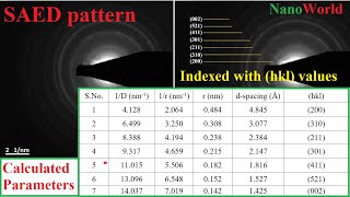
SAED, Selected Area Electron Diffraction Pattern: A Single Vs. Poly-crystalline Material

ฝัง
- เผยแพร่เมื่อ 21 ก.ย. 2024
- How to interpret Selected Area Electron Diffraction (SAED) graphs and HR-TEM/SAED graphs in your research paper or thesis?
SAED gives information whether your material is mono-crystalline, poly- crystalline or amorphous.
It gives the following information about the materials (Nanostructured Materials)
i. TEM is basically a nano size characterization tool.
ii. Shape and particle size (morphology, crystallite size, grain size, particle size, lattice information, plane indices, dislocations, and diffraction patterns)
iii. Grain boundaries


Thank you for this simple and concise explanation.
I am happy you like it. You are welcome
Great. Thank you, Sir. I appreciate you for your practical teaching.
Welcome
it's a best video for me studying about SAED. thanks.
Thank you, Sir, it's very informative, and I appreciate your enthusiasm for teaching and spreading knowledge
Welcome. I am glad it helps
Thank you so much for the comprehensive lecture! You made learning fun for me 😁
You are welcome 😊
I subscribed you on my first vist here, I am stingy in subscribing but i did subscribe your channel at my first visit. You have poured alot of knowledge here I am really thankful for that. Apart from that you are I think of my town side in Pakistan I have recongnized you from your speaking. Keep doing good work Doctor. Thank you
Thank you so much for supporting. Yes you are right.
very informative, I highly appreciate keep continue.
I am happy it helps. 🌹
Super video lot of hard work for giving excellent information
I am very happy it helps. Thanks for your nice words
Thank you sir.It is very informative.keep posting videos relating research ...
I am glad it help. Sure I will do. Thank you
thank you so much respected sir for giving precious information .. jazak Allah sir
You are always welcome
I appreciate your input.. really inspiring
Many thanks for your good words. 👍
X-Ray diffraction analyses would tell you whether the material is single-crystalline or poly-crystalline. In fact, in single-crystalline material, only one peak would be present. The peak intensity of the peaks also varies from powdered sample if texture is present. Similarly, in TEM analyses, if the beam covers multiple grains, which we usually observe during the diffraction of nanocrystalline material, we get spots from different grains and it may form rings.
Agreed. Single crystalline material gives sharp dots pattern while polycrystalline material gives sharp ring pattern. If the material is amorphous, it gives thick diffuse ring pattern.
Bro, poly-crystalline material also would give spot patterns. It often happens when the diameter of the grains falls within the micro-meter range, and those micron grain sized materials could be referred to as poly-crystalline. I agree if the grain size is smaller than the beam diameter or spot size which often leads to the diffraction of various grains simultaneously and produce rings. We often see rings in the case if nano sized precipitates are homogeneously distributed in the matrix.
@@arunbabuktkmce Agreed, good explanation. I just explained in broad the difference among the single and poly crystalline.
It is misguiding. If you use nano-crystalline instead of poly-crystalline, the result may be acceptable broadly
@@arunbabuktkmce I don't understand nono crystalline? Both single crystalline and polycrystlline are nanomaterials?? So what do you mean by that
Perfect explanation, subscribed.
You are always welcome.
love your videosss, make more vdeos like this on how to read graph of ceramicss
Thank you very much for your useful explanation.
You are welcome
Thank you sir for a very nice explanation.
I am happy it helps. Welcome
Thanks a lot for the explanations 😊
I am happy you like it. Thanks for watching my videos
Very Useful information, Thanks for the video. Please make videos for the characterization data interpretation
Thank you very much. Please see a lot of videos on this channel on characterization
come to the point yaar.
Excellent Sir.............
Love all videos..thank you Sir
I am happy it helps
Superb explanation
Thankful. I am so happy it helps
Thanks for the video. Can you also make a video on how to index the SAED using Gatan. Especially SAED of single crystal.
Thank you sir. Sure I will prepare
@@qamarwali am waiting for gatan microsuit for saed nd TEM image analysis. Howto download it??? Help me sir
Best vedio of the world
Many thanks 😊
awesome lecture video
Very helpful, thank you.
You are always welcome Sir
Sir I have one question if only circle is appear not in dots form then its crystalline or amorphous
If circled appear, then it's sure that the material is *polycrystalline*
If diffuse rings appear, then the material is *Amorphous*
Diffuse means the rings look blurred and not too visible
If dots appear but sharp dots, then it's sure the material is *Single-crystal*
If
Thanks for this video
You are welcome Sir.
Amazing sir g.....
Thanks
i wish we had laughter react in youtube🤣🤣🤣
Exactly. Thanks for watching
Thank you Mr
I need to know how to measure d spacing
Very easy. Will make video on it
Thank you Sir
You are welcome
Thanks for the video. How can I identify the crystallographic plane in a IFFT image? Since I don't have a SAED pattern image.
Welcome. FESEM can not tell us the crystallographic plan. Only SAED or XRD can confirm.
BTW what is IFFT?
Hi, You can do that using digital-micrograph software for IFFT and plane information. Just check any TH-cam video for downloading and using this software. Several videos are available! Thanks
Dear sir, looks-wise polycrystalline and amorphous SAED pics are very similar, how we differentiate them, please make on it also
Good question!. I think the SAED we uses for the crystalline materials whether it is single or polycrystlline. I am not sure about amorphous because in amorphous there is a complete disorder so I don't think this characterization tool will help.
How amorphous sturcture look likes in a picture?
The amorphous materials do not have any structure because the atoms are distributed in a complete disorder form as a result of no definite shape or structure
How to explain SAED pattern if it is diffused? Can we calculate lattice planes from it?
Yes sure. You can explain from it but I have just shown in this video just the difference between them
@@qamarwali Can you suggest me some reference on how to do it?
To be honest, I am not an expert of it. I have just shown in this video the difference between single and polycrystalline.
I am sure that there are a lot of materials and sources online.
zoom zoom zoom
Hi sir
How are you??
I am facing a problem in interpretation of SAED can you please provide your email? So i can discuss my problem with you
qamarwali@yahoo.com